Impedance Matching Networks
Posted: July 23, 2023
Overview:
- Investigate 2 element (L network) and 3 element (PI and T networks) impedance matching networks.
- Wideband matching network using cascaded L networks.
- Navigating the Smith Chart.
- 2 element and 3 element impedance matching using the Smith Chart.
Table of Contents
Introduction
Impedance matching is a useful tool that can be used to minimize reflections due to impedance discontinuities as well as maximize power transfer to a load (amplifier, antenna, etc.).
The maximum power transfer theorem states that the maximum power will be delivered from a source to its load if the load impedance is equal to the complex conjugate of the source impedance. Meaning, if you want to maximize power delivery to a load, the load impedance should have the same resistance as the source (real part of impedance) but opposite reactance of the source (imaginary part of impedance). With impedance matching we can force a load impedance to “look like” the complex conjugate of the source impedance so maximum power can be delivered.
RF Circuit Design looks at two methods of impedance matching:
- Impedance matching via equations.
- Impedance matching via Smith Chart.
Impedance Matching via Equations
L Network, 2 Element Network

Figure 1 - L Network
The L network is a simple 2 element matching network which got its name from the orientation and position of its 2 elements. There are 4 configurations of the L Network, seen in Figure 1, where configurations 1a) and 1c) form low-pass filters and configurations 1b) and 1d) form high-pass filters.
With L networks, the shunt element should be in parallel with the greater of the load resistor or source resistor. So configurations 1a) and 1b) would be used if the load resistor was greater than the source resistor and configurations 1c) and 1d) would be used if the source resistor was greater than the load resistor.
Therefore, the L network configuration will be determined by:
- Whether you want the network to act as a high-pass or low-pass filter.
- The resistance of the source and load impedance.
The L network functions by using the parallel element to transform the larger impedance down to a smaller value with equal resistance to the other terminating impedance while the series element resonates or cancels any reactance present in the network.
The elements in the L network are determined with the following equations:
$$Q_s = Q_p = \sqrt{\frac{R_p}{R_s} - 1}$$ $$Q_s = \frac{X_s}{R_s}$$ $$Q_p = \frac{R_p}{X_p}$$
Where:
\(Q_s\) = the Q of the series leg
\(Q_p\) = the Q of the shunt leg
\(R_s\) = the series resistance
\(R_p\) = the shunt resistance
\(X_s\) = the series reactance
\(X_p\) = the shunt reactance
The network elements can then be converted to capacitance and inductance with the following equations:
$$L = \frac{X}{\omega} = \frac{X}{2{\pi}f}$$ $$C = \frac{1}{{\omega}X} = \frac{1}{2{\pi}fX}$$
It should be noted that the L network is composed of frequency dependent reactive elements therefore a perfectly matched load from impedance matching will only occur at a single frequency.
L Network Design Example 1
Problem: Design a matching network for a circuit with a source resistance of 50 ohms and a load resistance of 250 ohms at 50 MHz. Assume DC voltage must be transferred to the load.
From the problem description above, configuration Figure 1a) must be chosen.
$$Q_s = Q_p = \sqrt{\frac{250}{50} - 1} = 2$$
$$X_s = (Q_s)(R_s) = (2)(50) = 100\;ohms$$
$$X_p = \frac{R_p}{Q_p} = \frac{250}{2} = 125\;ohms$$
$$L = \frac{X}{2{\pi}f} = \frac{100}{2{\pi}(50\mathrm{x}10^6)} = 318.3\;nH$$
$$C = \frac{1}{2{\pi}fX} = \frac{1}{2{\pi}(50\mathrm{x}10^6)(125)} = 25.5\;pF$$
We can then simulate our calculated network in QucsStudio as shown below.
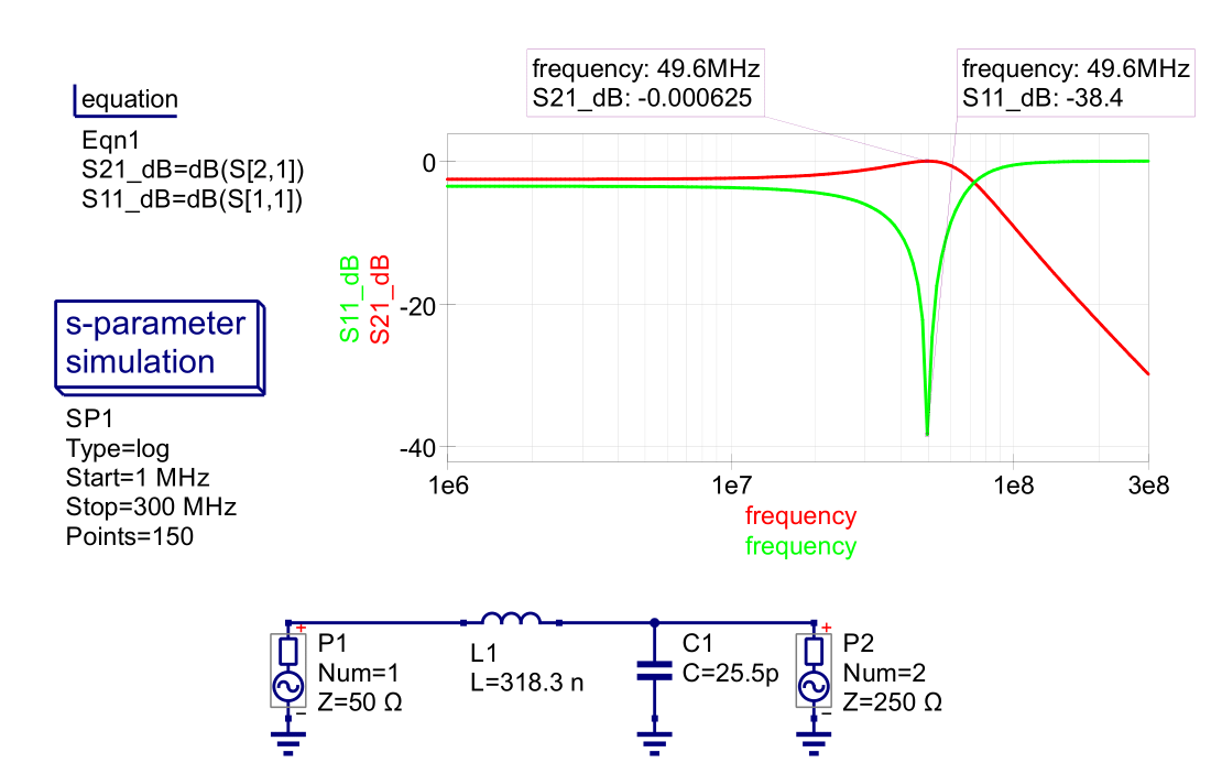
Figure 2 - L Network Example 1
L Network Design Example 2
Problem: Design a matching network for a circuit with a source resistance of 1000 ohms and a load resistance of 50 ohms at 50 MHz. Assume only AC voltage can be transferred to the load.
From the problem description above, configuration Figure 1d) must be chosen.
$$ Q_s = Q_p = \sqrt{\frac{850}{50} - 1} = 4 $$
$$ X_s = (Q_s)(R_s) = (4)(50) = 200\;ohms $$
$$ X_p = \frac{R_p}{Q_p} = \frac{850}{4} = 212.5\;ohms $$
$$ L = \frac{X}{2{\pi}f} = \frac{212.5}{2{\pi}(50\mathrm{x}10^6)} = 676.4\;nH $$
$$ C = \frac{1}{2{\pi}fX} = \frac{1}{2{\pi}(50\mathrm{x}10^6)(200)} = 15.9\;pF $$
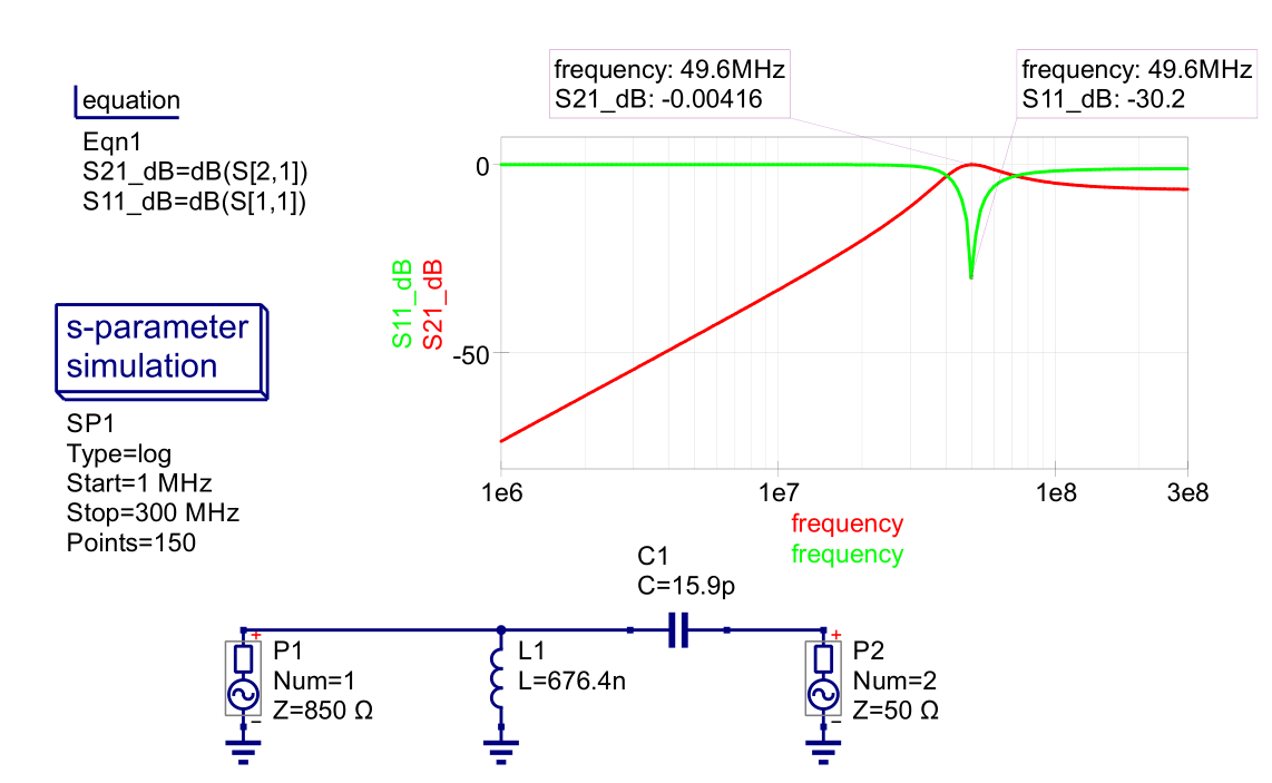
Figure 3 - L Network Example 2
L Networks with Complex Loads
RF Circuit Design discusses two approaches to dealing with complex source and load impedances:
- Absorption: Combining the stray reactance with the calculated matching network elements.
- Resonance: Resonate any stray reactance with an equal and opposite reactance at the desired frequency of interest.
The Absorption method involves using the same design process as with normal L networks with purely resistive loads but combing the stray component values into the matching network. This method will not work if the stray component value is larger than the calculated element value.
The Resonance method involves resonating away the stray reactance first so the source or load is purely resistive, then use the L matching network process above to match the two purely resistive loads.
The component value required to resonant the stray reactance at the resonant frequency can be determined by the following equations:
$$L = \frac{1}{\omega^2C}$$
$$C = \frac{1}{\omega^2L}$$
L Network Design Example 3
Problem: Design a matching network for the circuit in Figure 4 at 100 MHz. Assume only AC voltage can be transferred to the load.

Figure 4 - L Network with Complex Loads
Matching network configuration Figure 1b) will be used. To determine if the Resonance method is needed we will first calculate the network element values with purely resistive loads.
$$ Q_s = Q_p = \sqrt{\frac{400}{50} - 1} = 2.646 $$
$$ X_s = (Q_s)(R_s) = (2.646)(50) = 132.3\;ohms $$
$$X_p = \frac{R_p}{Q_p} = \frac{400}{2.646} = 151.2\;ohms $$
$$ L = \frac{X}{2{\pi}f} = \frac{151.2}{2{\pi}(100\mathrm{x}10^6)} = 240.6\;nH $$
$$C = \frac{1}{2{\pi}fX} = \frac{1}{2{\pi}(100\mathrm{x}10^6)(132.3)} = 12.03\;pF$$
We find that the stray capacitance in parallel with the load must be resonated away and the stray capacitance in series with the source can be absorbed.
The inductance required to resonate away the stray load capacitance at our desired matching frequency is,
$$L = \frac{1}{(2{\pi}(100\mathrm{x}10^6))^2(30\mathrm{x}10^-12)} = 84.4\;nH$$
When the shunt inductor calculated above is added, the load resistor becomes purely resistive. To handle the series capacitance at the source, we will absorb it into the calculated network capacitance above.
$$C = \frac{C_{total}C_{stray}}{C_{stray} - C_{total}} = \frac{(12.03\mathrm{x}10^{-12})(100\mathrm{x}10^{-12})}{(100\mathrm{x}10^{-12}) - (12.03\mathrm{x}10^{-12})} = 13.68\;pF$$
We can now assemble the matching network which is shown below.

Figure 5 - L Network with Complex Loads Matching Network
Finally, the network can be simplified further by combining the parallel inductors.
$$L_{total} = \frac{L_1L_2}{L_1 + L_2} = \frac{(240.6\mathrm{x}10^{-9})(84.4\mathrm{x}10^{-9})}{(240.6\mathrm{x}10^{-9}) + (84.4\mathrm{x}10^{-9})} = 62.5\;nH$$

Figure 6 - L Network with Complex Loads Matching Network Simplified
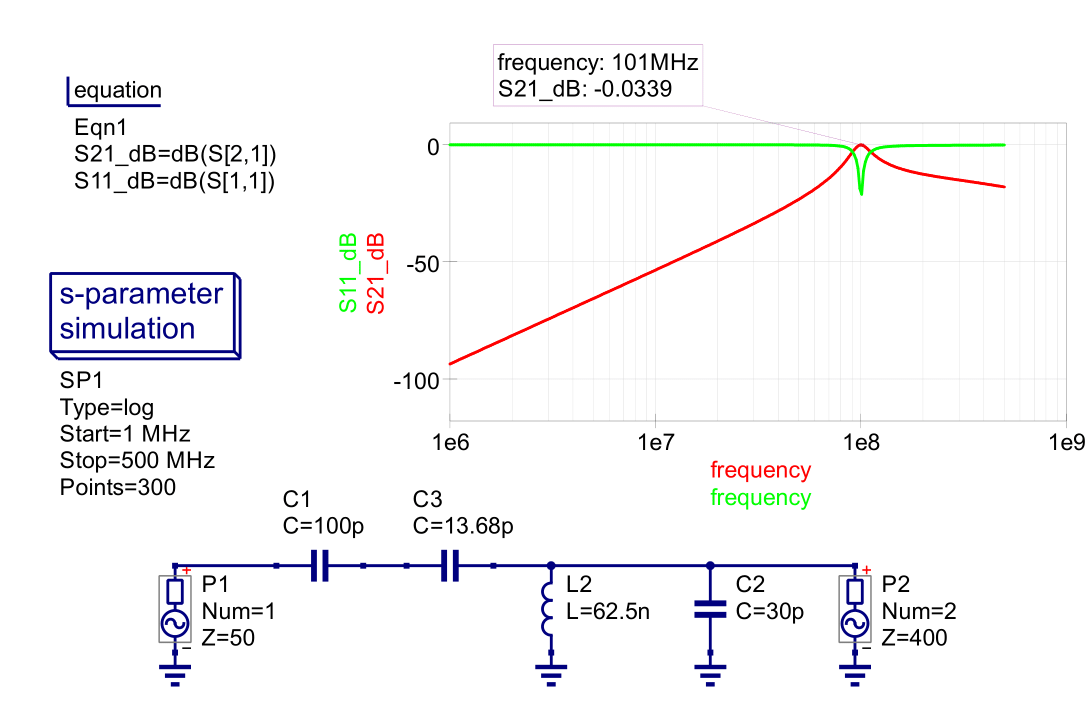
Figure 7 - L Network Example 3 Simulation
PI and T Networks, 3 Element Network
There are two 3 element matching networks, the PI network and T network. 3 element matching networks allows the designer to select the Q of the matching network. However, the Q of the 3 element matching network will be greater than the Q of an L network. Meaning the minimum circuit Q available for a 3 element network is that of a L networks.

Figure 8 - PI Network and T Network
As a reminder, the Q is the ratio of the network center frequency to its bandwidth and defined as:
$$Q = \frac{f_c}{f_{upper} - f_{lower}}$$
PI Network

Figure 9 - PI Network
The PI network can be broken down into two front to front L networks with a virtual resistance located between the two L networks
The negative sign for \(X_{S1}\) and \(X_{S2}\) are symbolic to indicate they are of opposite reactance of \(X_{P1}\) and \(X_{P2}\), respectively. For example, if \(X_{P1}\) is a capacitor, \(X_{S1}\) must be an inductor and if \(X_{P2}\) is an inductor, \(X_{S2}\) must be a capacitor.
When designing a PI network, the resistance of the virtual resistor must be smaller than either \(R_S\) or \(R_L\) because it is connected to the series arm. The exact value can be chosen by the desired Q of the circuit, where the Q is defined as,
$$Q = \sqrt{\frac{R_{large}}{R_{virtual}} - 1}$$
or
$$R_{virtual} = \frac{R_{large}}{Q^2+1}$$
Where $$R_{large} = \text{the largest terminating resistance of \(R_S\) or \(R_L\)}$$ $$R_{virtual} = \text{the virtual resistance}$$
It should be noted that in RF Circuit Design, it states that the equation is not entirely accurate, however it is a widely accepted Q-determining formula for this circuit, and is certainly close enough for most practical work.
PI Network Design Example 1
Problem: Design a PI matching network for a circuit with a source resistance of 50 ohms and a load resistance of 1000 ohms at 75 MHz. Assume the network must have a loaded Q of 18.
First find the virtual resistance.
$$R_{virtual} = \frac{R_{large}}{Q^2+1} = \frac{1000}{18^2+1} = 3.08\;ohms$$
Now we can find the element values on the load side.
$$ X_{P2} = \frac{R_{parallel}}{Q} = \frac{1000}{18} = 55.6\;ohms $$
$$ X_{S2} = (R_{series})(Q) = (3.08)(18) = 55.4\;ohms $$
We've now found the L network values on the load size. The Q for the L network on the source side is,
$$Q = \sqrt{\frac{50}{3.08} - 1} = 3.9$$
$$ X_{P1} = \frac{50}{3.9} = 12.8\;ohms $$
$$ X_{S1} = (3.08)(3.9) = 12.0\;ohms $$
We can now assemble the PI Network.

Figure 10 - PI Network Example 1
The component type can then be chosen depending on:
- Elimination of stray reactance, absorption or resonate.
- The need to filter high or low frequencies.
- Need to pass or block DC voltage.
- Availability of calculated component values.
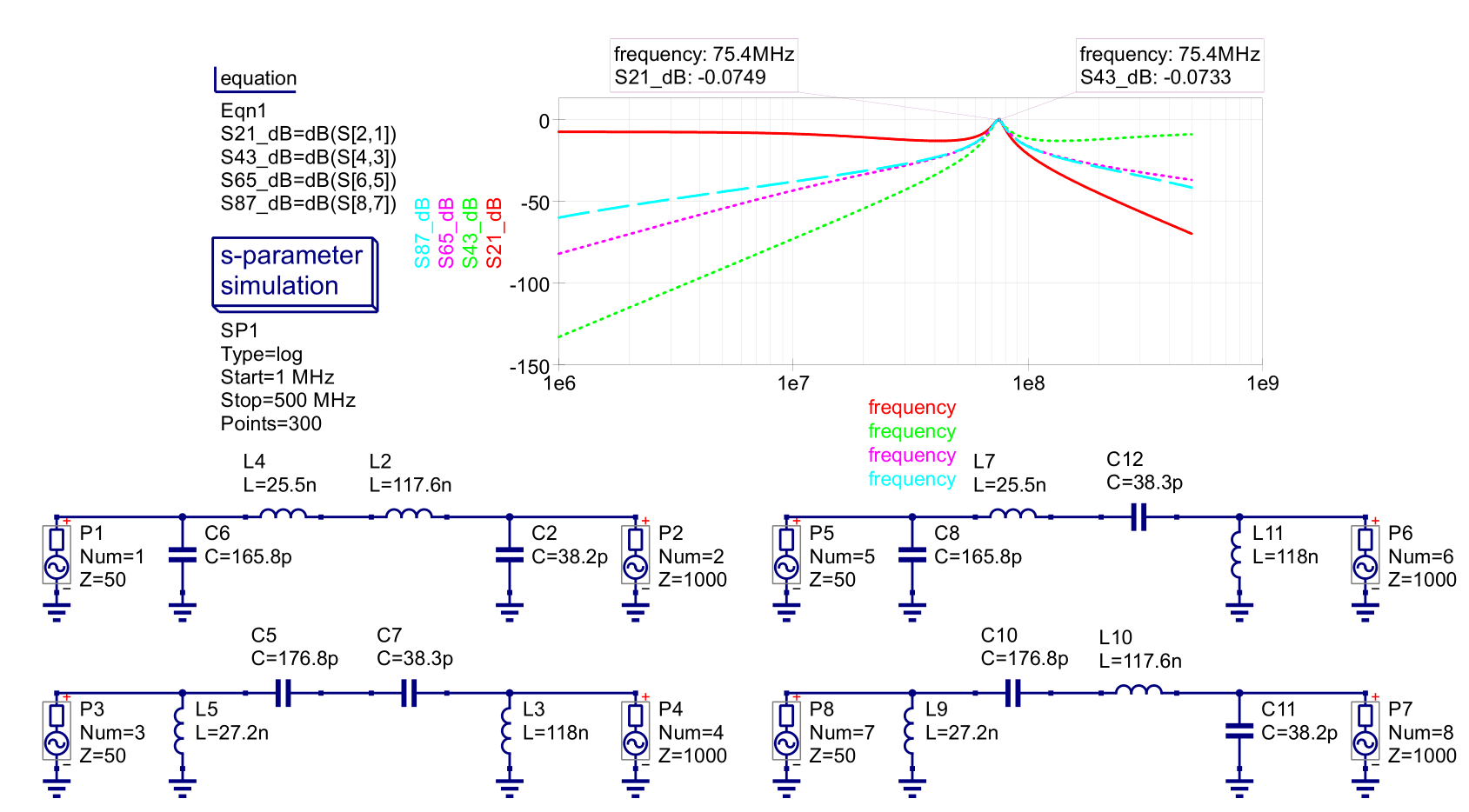
Figure 11 - PI Network Example 1 Simulation
The PI networks in Figure 11 can be simplified by combining the series elements.
T Network

Figure 12 - T Network
T networks can be described as two back to back L networks, where both shunt elements are connected together. In the T network, the virtual resistance should be larger than either the load or source resistance.
The T network is often used to match two low-valued impedances when a high-Q arrangement is needed. The loaded Q of the T network is determined by the L section that has the highest Q (which will be the end with the smallest terminating resistor).
In the T network, the Q is defined as:
$$Q = \sqrt{\frac{R_{virtual}}{R_{small}} - 1}$$
or
$$R_{virtual} = R_{small}(Q^2+1)$$
Where $$R_{small} = \text{the smallest terminating resistance of \(R_S\) or \(R_L\)}$$ $$R_{virtual} = \text{the virtual resistance}$$
T Network Design Example 1
Problem: Design a T matching network for a circuit with a source resistance of 10 ohms and a load resistance of 50 ohms at 50 MHz. Assume the network must have a loaded Q of 25.
First find the virtual resistance.
$$R_{virtual} = R_{small}(Q^2+1) = (10)(25^{2} + 1) = 6260\;ohms$$
Then calculate the L components for the source side:
$$ X_{P1} = \frac{6260}{25} = 250.4\;ohms $$
$$ X_{S1} = (25)(10) = 250\;ohms $$
Now find the loaded Q on the load side, then the L components:
$$Q = \sqrt{\frac{6260}{50} - 1} = 11.14$$
$$ X_{P2} = \frac{6260}{11.14} = 561.9\;ohms $$
$$ X_{S2} = (11.14)(50) = 557\;ohms $$
We can now assemble the T network with the component values calculated above:

Figure 13 - T Network Example 1
Like the PI network, the component type will be chosen for the same rules as those specified in PI Network Example 1. The T networks in Figure 14 can be simplified by combining the parallel elements.
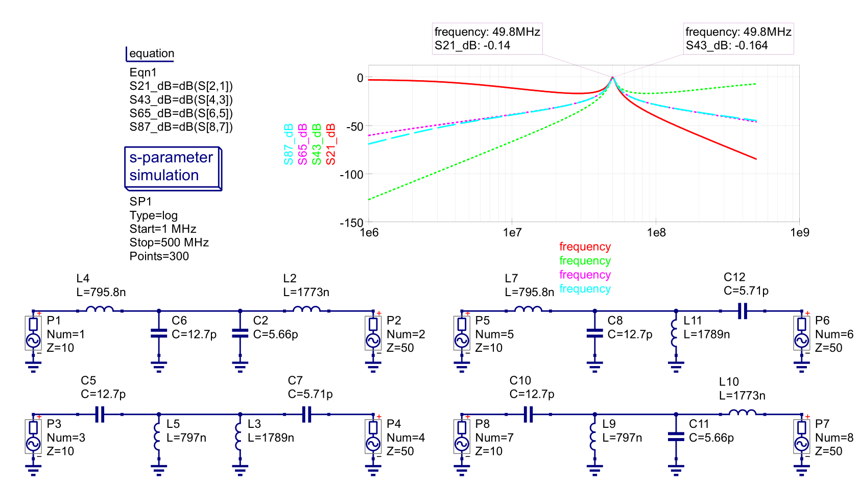
Figure 14 - T Network Example 1 Simulation
Wideband Matching Network
How do we handle applications where we need matching over a broad range of frequnecies? Or in other words, how can we build a low-Q matching network? We can simply use multiple L networks connected in series meaning the virtual resistor is in shunt with one L network while in series with the other.

Figure 15 - Wideband Networks
With the multistage L network configuration, the virtual resistor must be larger than the smallest termination resistance and, smaller than the largest termination resistance.
The maximum bandwidth (minimum Q) available from the two stage L network is obtained when the virtual resistor is made equal to the geometric mean of the two impedances being matched.
$$R_{virtual} = \sqrt{R_SR_L}$$
The loaded Q is then:
$$Q = \sqrt{\frac{R_{large}}{R_{virtual}} - 1} = \sqrt{\frac{R_{virtual}}{R_{smaller}} - 1}$$
If even wider bandwidths are needed, more L networks may be cascaded together with virtual resistances between each stage. Optimum bandwidths in these cases are obtained if the ratios of each of the two succeeding resistances are equal:
$$\frac{R_{1}}{R_{smaller}} = \frac{R_{2}}{R_{1}} = \frac{R_{3}}{R_{2} }... = \frac{R_{larger}}{R_{n}} $$
Where \(R_1, R_2, R_3 ... R_n\) are the virtual resistors.
Wideband Network Design Example 1
Problem: Design a two stage wideband matching network for a circuit with a source resistance of 10 ohms and a load resistance of 500 ohms at 50 MHz. Loaded Q shall be chosen for maximum bandwidth. Assume DC must be delivered to the load.
First find virtual resistance for maximum bandwidth Q.
$$R_{virtual} = \sqrt{(10)(500)} = 70.71\;ohms$$
Therefore
$$Q = \sqrt{\frac{500}{70.71} - 1} = \sqrt{\frac{70.71}{10} - 1} = 2.46$$
We can now calculate the L network component values. First start with source side:
$$ X_{P1} = \frac{70.71}{2.46} = 28.74\;ohms $$
$$ X_{S1} = (2.46)(10) = 24.6\;ohms $$
$$ X_{P2} = \frac{500}{2.46} = 203.3\;ohms $$
$$ X_{S2} = (2.46)(70.71) = 173.9\;ohms $$
Because DC must be delivered to the load, the series elements shall be inductors.
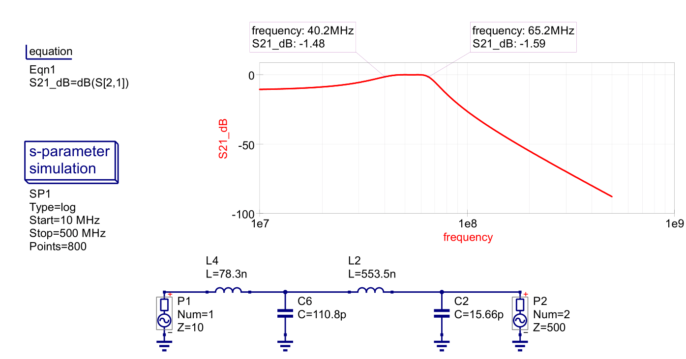
Figure 16 - Wideband Network Example 1 Simulation
If we calculate the Q from the simulated data, using the 1.5-dB points for the upper and lower frequencies (3-dB for voltage ratio), the Q is around 2.0. Not sure why the Qs differ significantly, could be inaccuracy of equation but will have to investigate further.
Wideband Network Design Example 2
Problem: Design a multistage stage wideband matching network for a circuit with a source resistance of 10 ohms and a load resistance of 500 ohms at 50 MHz. Ensure loaded Q is no greater than 1. Assume DC must be delivered to the load.
We will design for a Q of around 0.8 to give us a safety margin to not go over 1. Let's first find the virtual resistance on the load side:
$$R_{virtual1} = \frac{R_{load}}{Q^2+1} = \frac{500}{{0.8}^2+1} = 304.9$$
We can use the same equation above until we find a virtual resistance which is less than our source resistance which will determine the number of stage that is required.
$$R_{virtual2} = \frac{R_{vitual1}}{Q^2+1} = \frac{304.9}{{0.8}^2+1} = 185.9\;ohms$$
$$R_{virtual3} = \frac{R_{vitual2}}{Q^2+1} = \frac{185.9}{{0.8}^2+1} = 113.4\;ohms$$
$$R_{virtual4} = \frac{R_{vitual3}}{Q^2+1} = \frac{113.4}{{0.8}^2+1} = 69.1\;ohms$$
$$R_{virtual5} = \frac{R_{vitual4}}{Q^2+1} = \frac{69.1}{{0.8}^2+1} = 42.1\;ohms$$
$$R_{virtual6} = \frac{R_{vitual5}}{Q^2+1} = \frac{42.1}{{0.8}^2+1} = 25.7\;ohms$$
$$R_{virtual7} = \frac{R_{vitual6}}{Q^2+1} = \frac{25.7}{{0.8}^2+1} = 15.7\;ohms$$
$$R_{virtual8} = \frac{R_{vitual7}}{Q^2+1} = \frac{15.7}{{0.8}^2+1} = 9.57\;ohms$$
We find that the eighth virtual resistance is lower than our source resistor so we only need 7 virtual resistors. The Q of the source L network will be,
$$Q = \sqrt{\frac{15.7}{10} - 1} = 0.755$$
We can now calculate the element values for each of the 8 L networks,
$$ X_{P1} = \frac{15.7}{0.755} = 20.8\;ohms $$
$$ X_{S1} = (0.755)(10) = 7.55\;ohms $$
$$ X_{P2} = \frac{25.7}{0.8} = 32.1\;ohms $$
$$ X_{S2} = (0.8)(15.7) = 12.6\;ohms $$
$$ X_{P3} = \frac{42.1}{0.8} = 52.6\;ohms $$
$$ X_{S3} = (0.8)(25.7) = 20.6\;ohms $$
$$ X_{P4} = \frac{69.1}{0.8} = 86.4\;ohms $$
$$ X_{S4} = (0.8)(42.1) = 33.7\;ohms $$
$$ X_{P5} = \frac{113.4}{0.8} = 141.8\;ohms $$
$$ X_{S5} = (0.8)(69.1) = 55.3\;ohms $$
$$ X_{P6} = \frac{185.9}{0.8} = 232.4\;ohms $$
$$ X_{S6} = (0.8)(113.4) = 90.7\;ohms $$
$$ X_{P7} = \frac{304.9}{0.8} = 381.1\;ohms $$
$$ X_{S7} = (0.8)(185.9) = 148.7\;ohms $$
$$ X_{P8} = \frac{500}{0.8} = 625\;ohms $$
$$ X_{S8} = (0.8)(304.9) = 243.9\;ohms $$
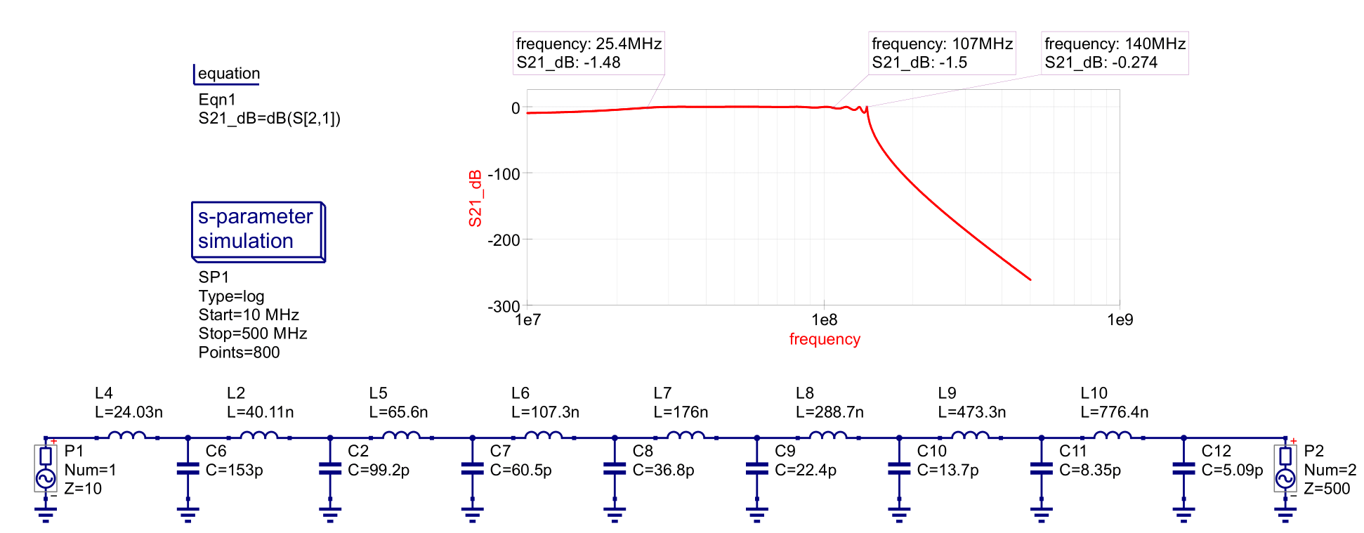
Figure 17 - Wideband Network Example 2 Simulation
From the above S21 data, we find that our wideband matching network takes the shape of a sharp LPF with a cutoff around 140 MHz. Our matching network also has ripple near the cutoff frequency similar to Chebyshev filter. So perhaps a lower order LPF using less components may be a better solution for our problem.
The Smith Chart
Navigating the Smith Chart
The Smith Chart can be drawn to represent impedance \(Z\), admittance \(Y = \frac{1}{Z}\) or both impedance and admittance. The impedance Smith Chart is made up of constant resistance \(R\) circles and constant reactance \(X\) circles while the admittance Smith Chart is made up of constant conductance \(G\) circles and constant susceptance \(B\) circles.
The designer can switch between impedance and admittance by simply measuring the distance d from the impedance or admittance to the center of the chart then plotting the result the same distance from the center but in the opposite direction.
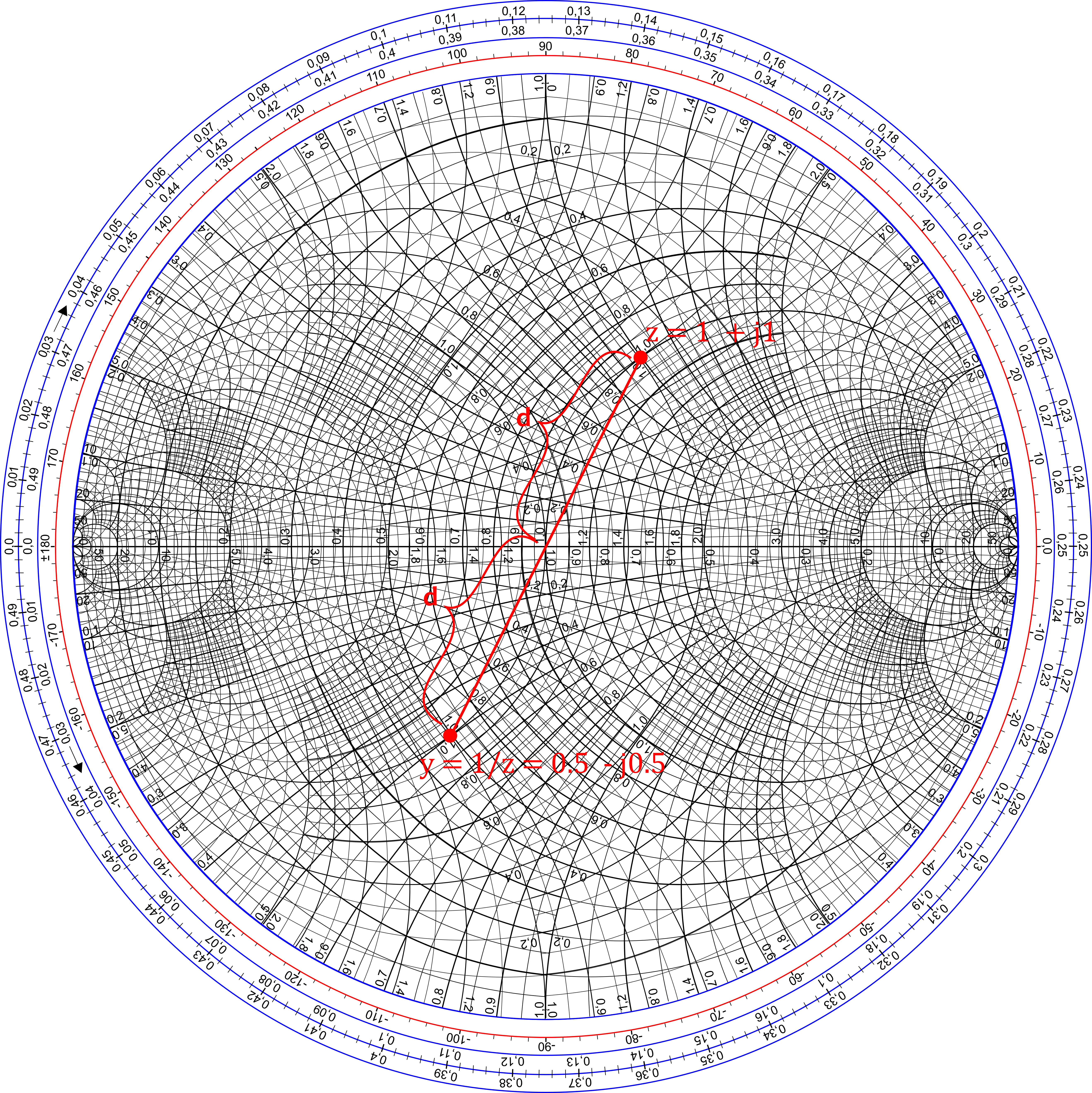
Figure 18 - Impedance To Admittance
Values plotted on the Smith Chart are normalized first. This means all impedances plotted will first be divided by some convenient number such as the characteristic impedance of your transmission line or source/load impedance.
Because circles cannot be drawn for every resistance and reactance values, impedances may need to be plotted in inexact locations and therefore can cause small errors.
The book outlines an easy way of navigating the Smith Chart when adding series and shunt L or C components without needing to change between impedance and admittance.
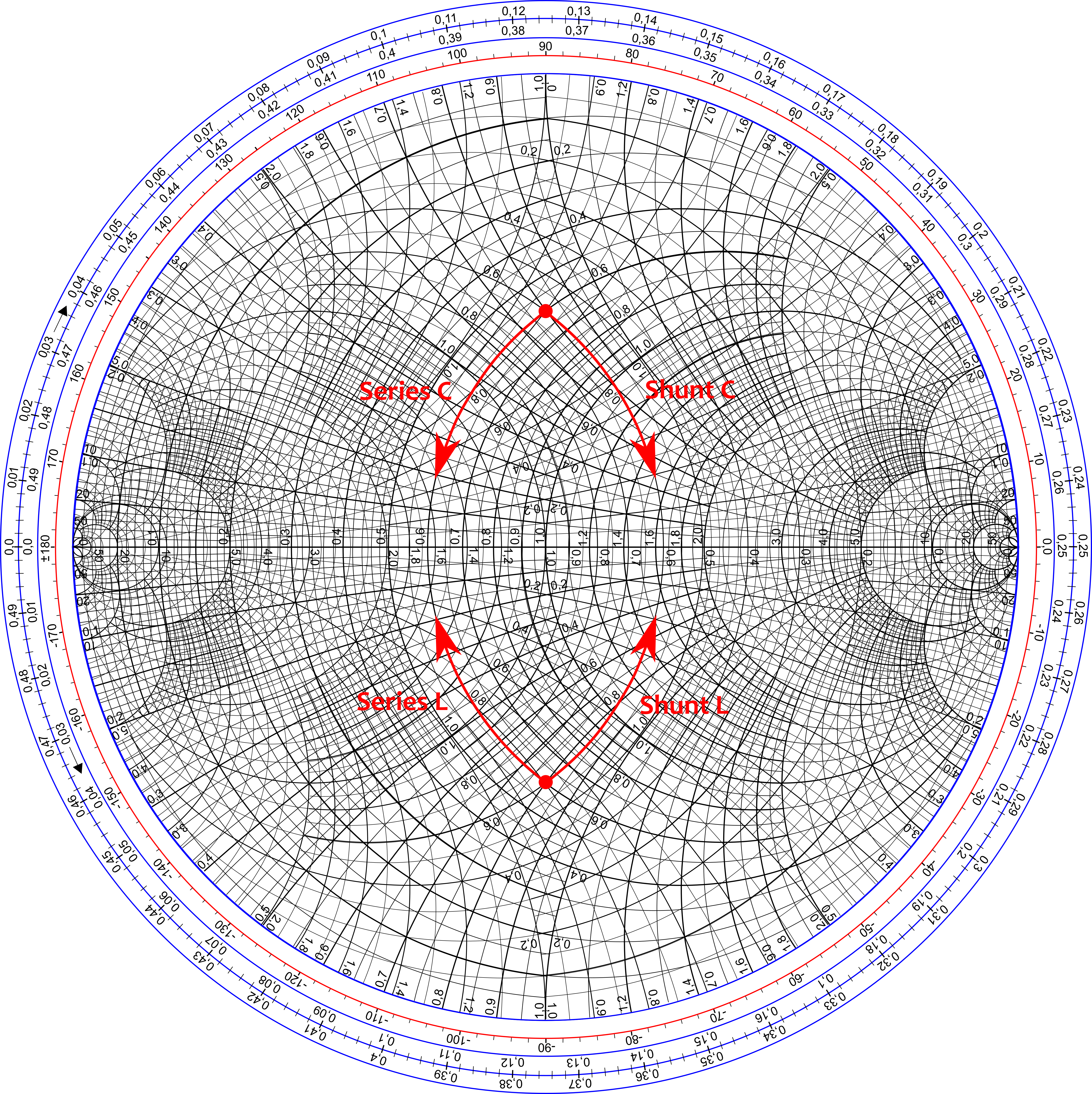
Figure 19 - Impedance and Admittance Chart Navigation
Smith Chart Example 1
Problem: Using a Smith Chart, find the impedance looking into the network shown in Figure 20a).

Figure 20 - Smith Chart Example 1
The network in Figure 20a) can be broken down into individual components as shown in Figure 20b). We can plot the first impedance, the load impedance, then work backwards towards the source. First we plot the impedance seen from point A, \(Z = 1 + j1\;ohm\), then add the following component until point E.
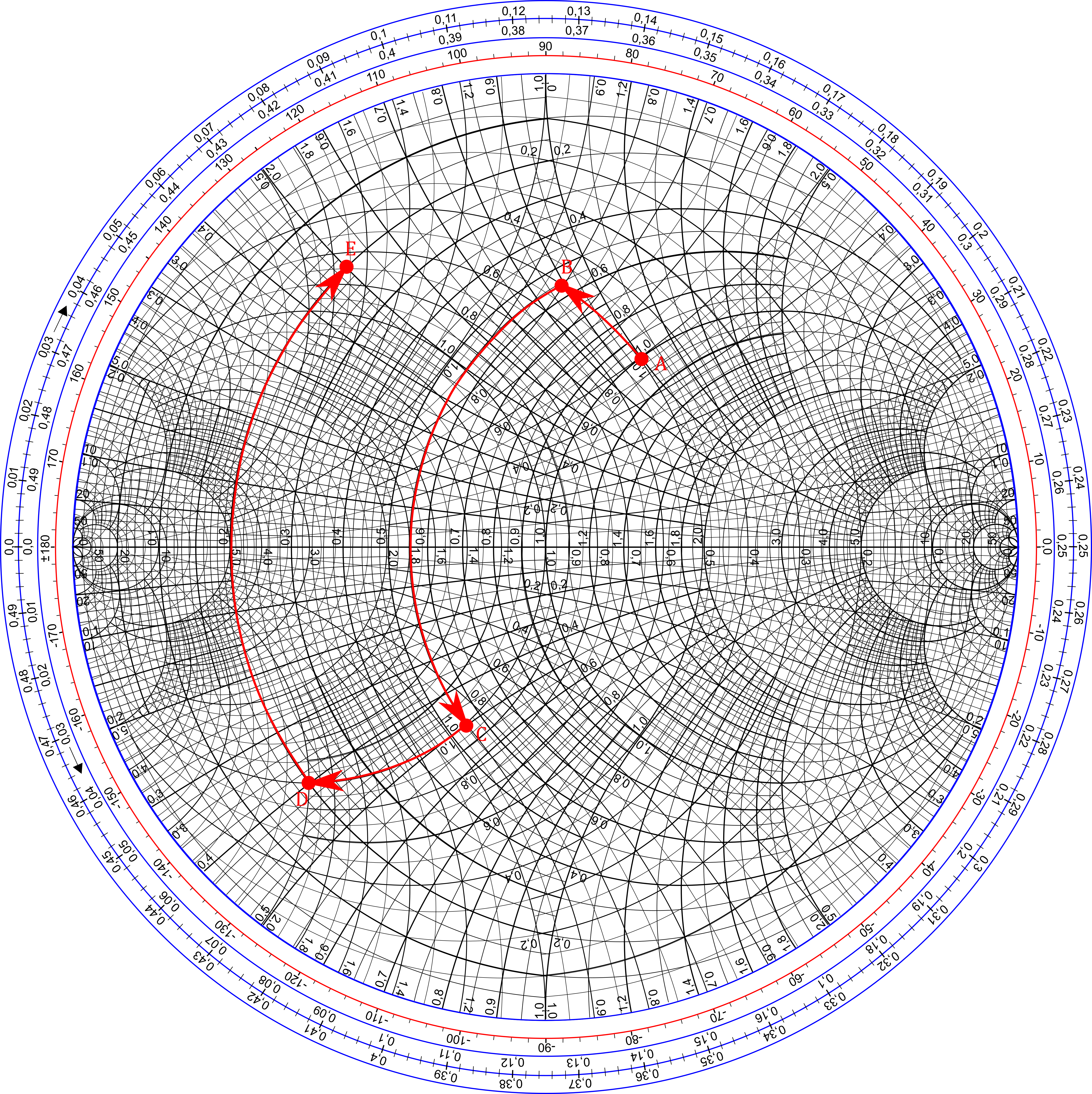
Figure 21 - Smith Chart Example 1 Impedance Only
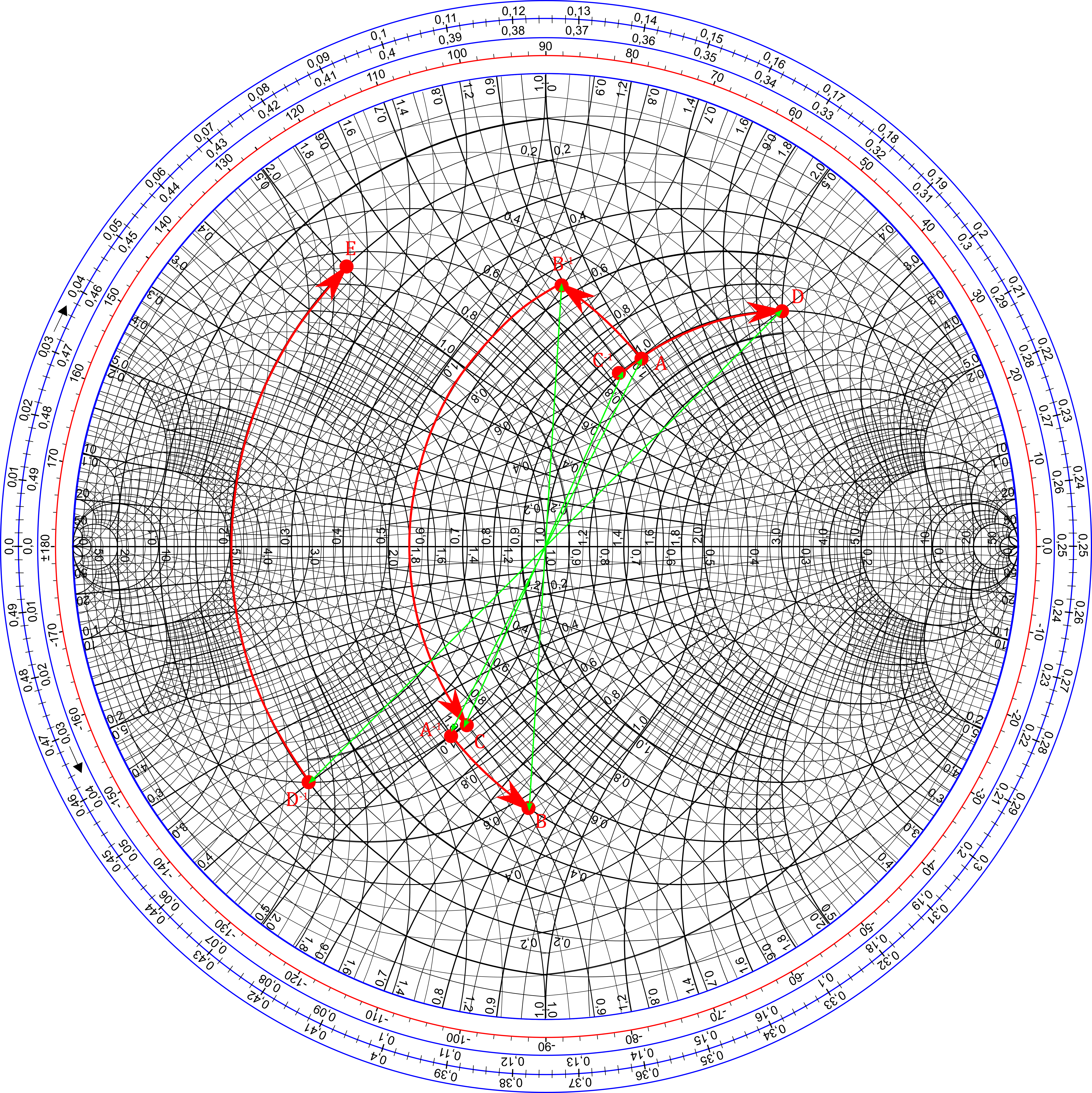
Figure 22 - Smith Chart Example 1 Impedance and Admittance
We see that either switching between impedance and admittance charts or staying within the impedance chart results in the same overall network impedance of \(Z = 0.2 + j0.5\;ohm\)
Smith Chart Impedance Matching
2 Element Matching with the Smith Chart
To design an impedance matching network with the Smith Chart we simply plot the load impedance and begin adding series and shunt elements until we reach the complex conjugate of the source impedance.
When plotting elements on the Smith Chart, we can convert the reactance and susceptance to it's L and C component values with the following equations:
Series C element:
$$C = \frac{1}{2{\pi}fXN}$$
Series L element:
$$L = \frac{XN}{2{\pi}f} $$
Shunt C element:
$$C = \frac{B}{2{\pi}fN}$$
Shunt L element:
$$L = \frac{N}{2{\pi}fB} $$
where:
\(X\) = the reactance from the chart
\(B\) = the susceptance from the chart
\(N\) = the number used to normalize the chart impedance
Smith Chart Matching Network Example 1
Problem: Using a Smith Chart, design a 2 element matching network for a circuit with a source resistance of 50 - j15 ohms and a load resistance of 100 + j25 ohms at 80 MHz. Assume DC voltage must be transferred to the load.
We will first plot our normalized load impedance and normalized complex conjugate source impedance on the Smith Chart. We can then work backwards from the load impedance towards the normalized complex conjugate source impedance by adding series and parallel elements. If we choose N = 50, our normalized source impedance will be \(z_S = 1 - j0.3\) and the normalized load impedance will be \(z_L = 2 + j0.5\).
Because the load resistance is greater than the source resistance and DC voltage must be delivered to the load, our first element added will be a shunt capacitor in parallel with the load followed by a series inductor.
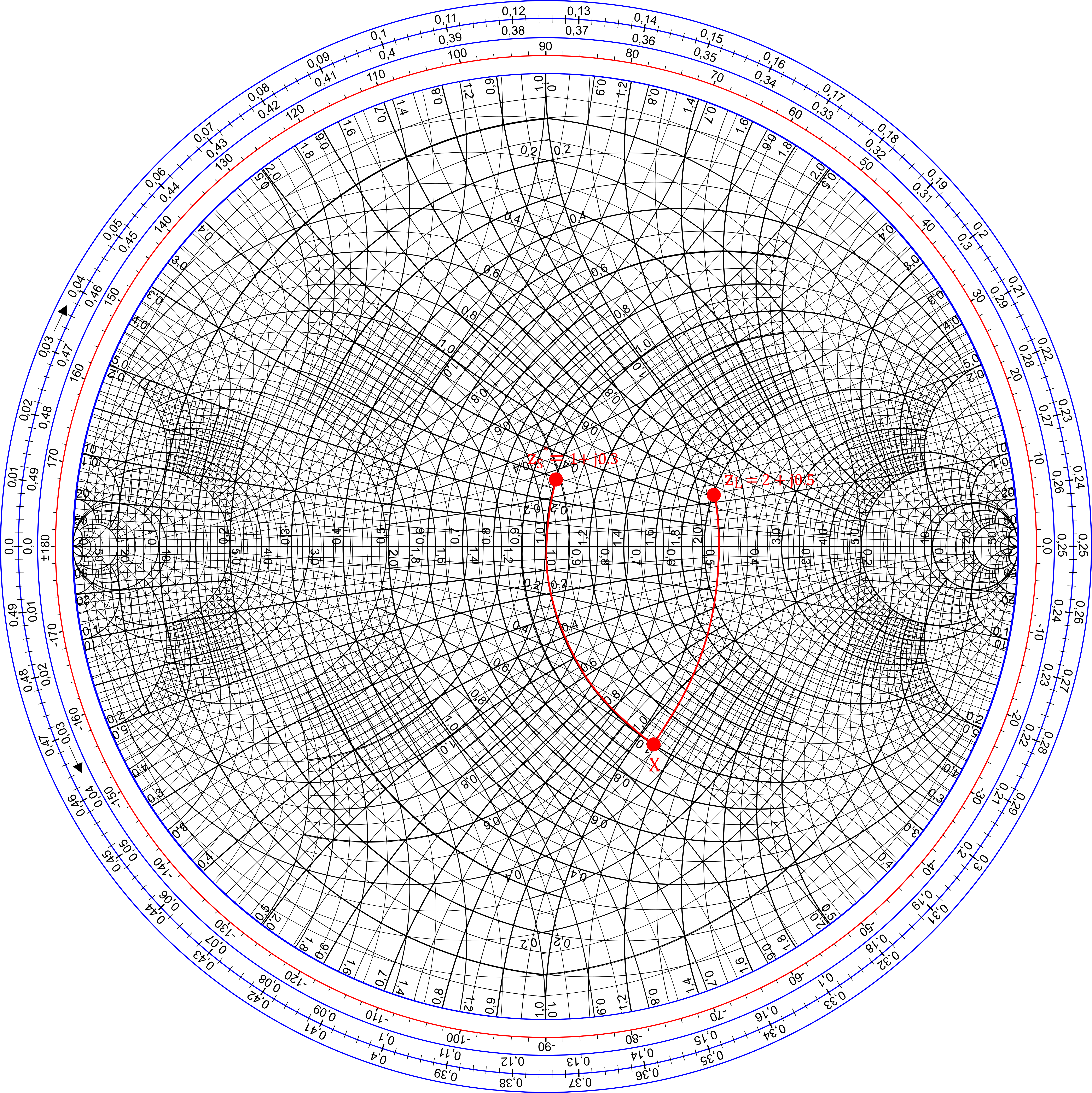
Figure 23 - Smith Chart Matching Network Example 1
We find the shunt capacitor has a value of +jB = 0.62 mhos and the series inductor has a value of +jX = 1.38 ohms.
Using the previous equations, we can find the L and C component values:
$$C = \frac{B}{2{\pi}fN} = \frac{0.62}{2{\pi}(80\mathrm{x}10^6)(50)} = 24.67\;pF$$
$$L = \frac{XN}{2{\pi}f} = \frac{(1.38)(50)}{2{\pi}(80\mathrm{x}10^6)} = 137.2\;nH$$
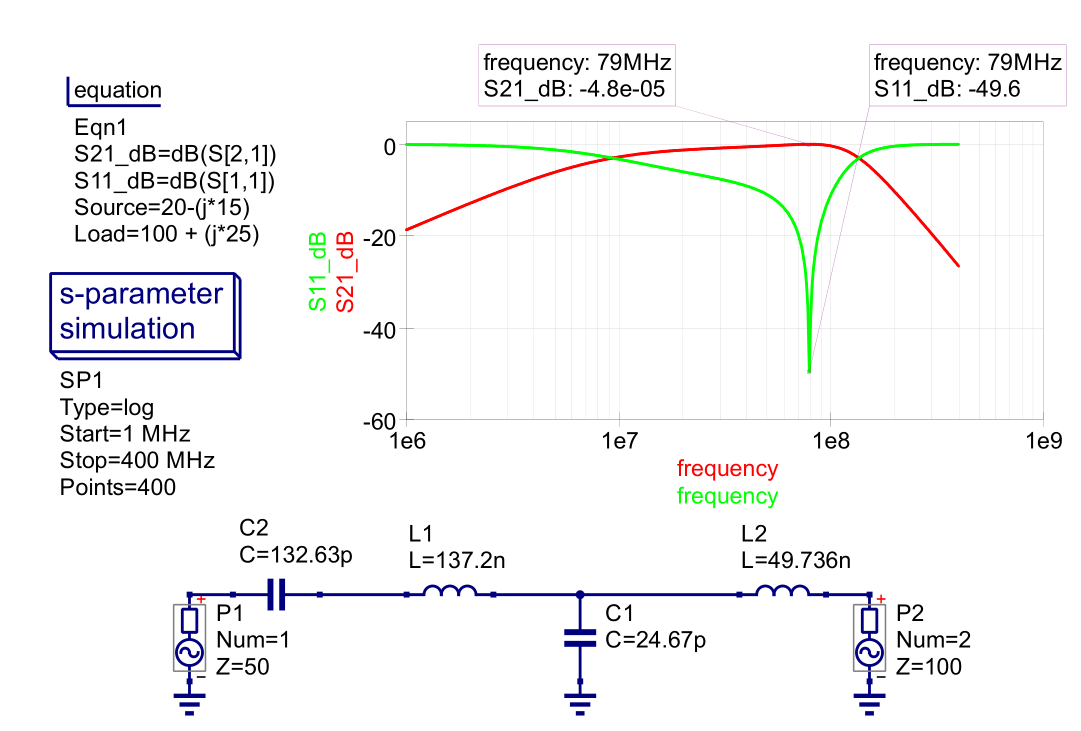
Figure 24 - Smith Chart Matching Network Example 1 Simulation
It should be noted that components C2 and L2 are the reactance portion of the source and load impedance, respectively. QucsStudio was unable to compute complex impedances for the Power Source element (P1 and P2) and specifying the complex impedance as a variable using the Equation block did not work either.
3 Element Matching with the Smith Chart
As mentioned earlier, with a 3 element network the loaded Q of the network can be chosen.
The Q at any point on the Smith Chart representing a series network can be calculated by taking the ratio of its reactance to its resistance. Therefore, for any Q there will be an infinite number of combinations of reactance and resistance that meets that Q value. These constant Q line are represented as arcs from the open circuit point to the short circuit point on the Smith Chart. Where the arc along the perimeter of the Smith Chart characterizes an infinite Q and the pure resistance line across the center of the chart represents a Q of 0.
The procedure for designing a three-element impedance matching network for a specified Q is summarized as follows:
- Plot the constant Q arc for the desired Q.
- Plot the load impedance and the complex conjugate of the source impedance.
- Determine the network type (PI or T) and the end of the network that will be used to set the Q of the network. As a reminder, for T networks, the end with the smaller terminating resistance determines the Q and for PI networks, the end with the larger terminating resistance determines the Q.
- Intersect the constant Q arc with the added network element on the end that determines the Q.
An example of Step 4 above is if \(R_L\) is greater than \(R_S\) and a PI network is used, then the point between the first added element's arc and the second added elements arc should lie on the desired constant Q arc. If a T network is used instead, then the point between the second added element's arc and the third added elements arc should lie on the desired constant Q arc.
Smith Chart Matching Network Example 2
Problem: Using a Smith Chart, design a 3 element matching network for a circuit with a source resistance of 50 - j15 ohms and a load resistance of 100 + j25 ohms at 80 MHz. Assume DC voltage must be transferred to the load and a network Q of 10.
We'll use the PI network with two shunt capacitors and a series inductor. The load resistance is greater than the source resistance, therefore the load side will determine the Q.
We'll use the same normalized source impedance \(z_S = 1 - j0.3\) and the normalized load impedance \(z_L = 2 + j0.5\) with N = 50 as found in Example 1.
We can now plot our normalized impedances and begin adding our elements starting from the load until the complex conjugate of the source impedance is reached. We must also ensure to end the arc of our first element on the desired constant Q line.
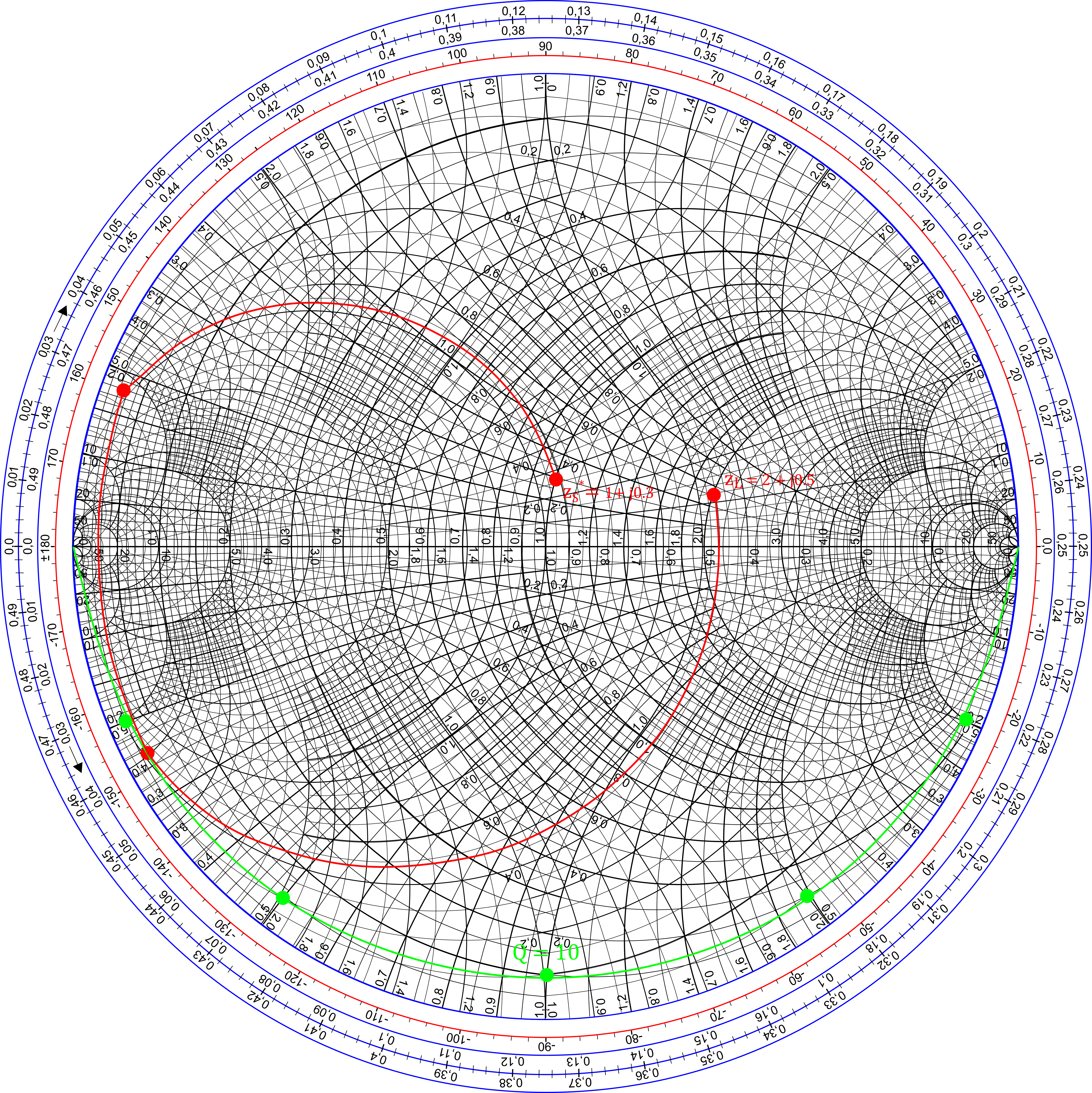
Figure 25 - Smith Chart Matching Network Example 1
We find the first shunt capacitor has a value of +jB = 4.12 mhos, the series inductor has a value of +jX = 0.425 ohms and second shunt capacitor has a value of +jB = 6.23 mhos.
The component values are
$$C_1 = \frac{B}{2{\pi}fN} = \frac{4.12}{2{\pi}(80\mathrm{x}10^6)(50)} = 163.9\;pF$$
$$L_1 = \frac{XN}{2{\pi}f} = \frac{(0.425)(50)}{2{\pi}(80\mathrm{x}10^6)} = 42.28\;nH$$
$$C_2 = \frac{B}{2{\pi}fN} = \frac{6.23}{2{\pi}(80\mathrm{x}10^6)(50)} = 247.9\;pF$$
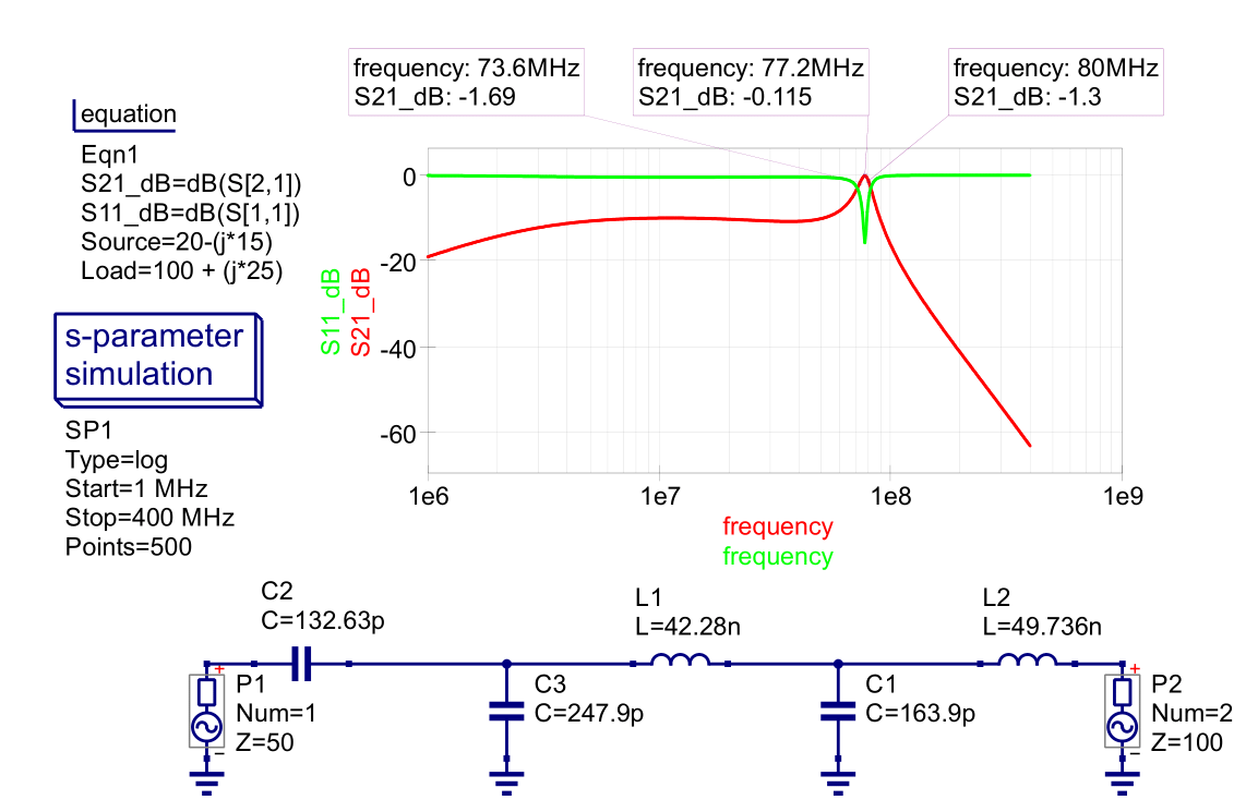
Figure 26 - Smith Chart Matching Network Example 2 Simulation
Again, C2 and L2 of the figure above are the reactance portion of the source and load impedance, respectively. We find that using the component values determined by the Smith Chart, we achieve minimum insertion loss at 77.2 MHz (slightly off from our desired 80 MHz) and a Q of around 12 when using 1.5 dB points for the upper and lower frequencies.
Practical Example
Suppose we are designing a narrow-band transceiver for operation at 5.75 GHz. We may decide to use a small form factor chip antenna for our transceiver, such as the Johanson Technology 5500AT18A0725.
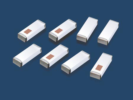
Figure 27 - Chip Antenna
However, we find that this antenna's return loss (S11) is slightly too high at our desired frequency. Well, this is a perfect situation in which we can use impedance matching to increase the power delivered to the antenna and thus decrease our return loss.
In our design we'll just use a simple L network to match our source impedance to our antenna. Our source could be our transceiver or an external amplifier. From the S1P model of our chip antenna, we can find its series impedance by inspecting the S11 trace (blue trace) on the Smith Chart at 5.75 GHz, seen in Figure 28. We find its impedance at 5.76 GHz is \(Z_L = 29.4\angle1.78^\circ\) or in rectangular form \(Z_L = 29.39 + j0.913\:ohms\). Assuming our source impedance is 50 ohms we can begin designing our matching network.
We wish to only pass AC voltage to our antenna and because our source resistance is larger than our load resistance, the parallel inductor will be on the source side.
$$Q_s = Q_p = \sqrt{\frac{50}{29.39} - 1} = 0.837$$
$$X_s = (Q_s)(R_s) = (0.837)(29.39) = 24.60\;ohms$$
$$X_p = \frac{R_p}{Q_p} = \frac{50}{0.837} = 59.74\;ohms$$
We will combine the series reactance component of the load (antenna) with our series element therefore our series element after absorption is 23.687 ohms. We can then calculate our L and C component values.
$$L = \frac{59.74}{2{\pi}(5.75\mathrm{x}10^9)} = 1.651\;nH$$
$$C = \frac{1}{2{\pi}(5.75\mathrm{x}10^9)(23.687)} = 1.167\;pF$$
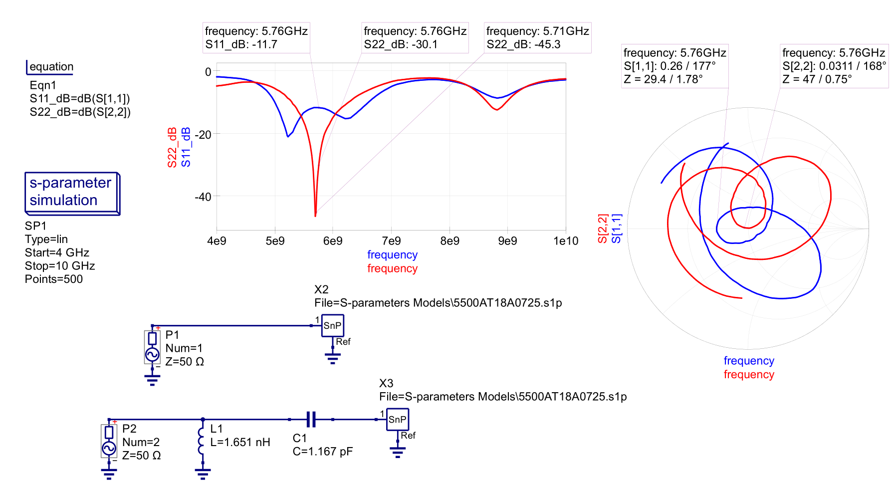
Figure 28 - Chip Antenna Matching Network
How much additional power is delivered to the antenna when using this matching network, assuming lossless components and transmission lines? From Figure 28, we find our return loss is -11.7 dB without the matching network and -30.1 dB with the matching network at 5.75 GHz. Assuming our output delivers 1 watt to the antenna then:
$$\Gamma_{no\,matching} = 10^{-11.7/20} = 0.26$$
$$\Gamma_{matching} = 10^{-30.1/20} = 0.0313$$
$$P_{reflected\,no\,matching} = \Gamma_{no\,matching}^2P_{forward} = (0.26)^2(1 W) = 67.6\;mW$$
$$P_{reflected\,matching} = \Gamma_{matching}^2P_{forward} = (0.0313)^2(1 W) = 0.98\;mW$$
So an additional 66.62 mW is delivered to the antenna instead of being reflected back. Now it is up to the designer to determine if this additional power delivered to the antenna and minimized reflections is worth sacrificing a wider bandwidth and extra cost of matching components.
References
Chris Bowick, RF Circuit Design, Second Edition, 2008, https://ia801604.us.archive. org/21/items/RFCircuitDesign2ndEdition/RF%20Circuit%20Design%20-%202nd%20Edition.pdf