LC Filter Design Using Normalized Prototypes
Posted: Aug. 21, 2023
Overview
- Create an LC Low-Pass Filter (LPF), High-Pass Filter (HPF) and Bandpass Filter (BPF) from a normalized low-pass prototypes.
- Use Response Transformation to convert normalized LPFs to HPFs and BPFs.
- Use Frequency and Impedance scaling to set desired load resistances and cutoff frequencies.
Table of Contents
- Introduction
- Choosing a Normalized Low-Pass Filter
- Response Transformation
- Frequency and Impedance Scaling
- Low-Pass Filter Example
- High-Pass Filter Example
- Bandpass Filter Example
Introduction
The days of designing LC filters from scratch are no longer. A modern method to design LC filters are software tools found online or in Electronic Design Automation (EDA) software. Another method is using normalized low-pass filter prototypes. In this method, the procedure starts with determining the requirements then finding a filter in a catalog that satisfies these requirements. The normalized element values of the chosen filter can then be transformed to the type of response we wish (no transformation required for LPFs) and finally scaled to the desired cutoff frequency and source/load resistances.
Choosing a Normalized Low-Pass Filter
In order to standardize the catalog of filters to easily compare filter types and orders, normalization is often implemented. Most catalogued filters are low-pass filters normalized for a cutoff frequency of 1 rad/s (0.159 Hz) with a source and load resistance normalized so \(R_L\) equals 1 ohm. This normalized filter is sometimes referred to as a low-pass prototype.
With the catalogue of filter prototypes, we can easily compare then choose a filter that meets our requirements. The specifications of a filter can include the following:
- Passband ripple or no ripple
- Attenuation steepness
- Number of filter elements
- Ratio between source resistance to load resistance
- Group delay characteristics
When choosing a filter prototype for a HPF, the attenuation characteristics will be mirrored at the cutoff frequency. For example, if the attenuation characteristics for a normalized LPF is 40 dB when \(f/f_c\) equal 3 (3 times cutoff) then when transformed the filter will have the same attenuation, 40 dB, when \(f/f_c\) equals 1/3.
When designing a BPF, we first need to find our ratio of bandwidths
$$ BW_{XdB}/BW_{3dB} $$
where:
\(BW_{XdB}\) = the bandwidth at the required attenuation level
\(BW_{3dB}\) = the 3-dB bandwidth of the bandpass filter
Then we find a LPF prototype where \(f/f_c\) is our desired attenuation at \(BW_{XdB}/BW_{3dB}\). For example, if our 60-dB bandwidth \(BW_{60dB}\) is 40 MHz and our 3-dB bandwidth \(BW_{3dB}\) is 10 MHz. We would need to find a prototype where the attenuation characteristics is 60-dB minimum at \(f/f_c\) = \(BW_{60dB}/BW_{3dB}\) = 4.
When choosing a LPF prototypes, we typically want to minimize the number of inductors in the filter. Real inductors typically have a lower-Q than capacitors (higher losses) therefore degrade the overall performance of the filter. This should also be kept in mind when transforming a LPF to a HPF or BPF.
Once a LPF prototype is chosen based on our criteria, we can move on to transformation or scaling the LPF prototype to our desired source and load resistance as well as our desired cutoff frequency.
Response Transformation
When designing HPFs or BPFs the normalized LPF prototype must be transformed to our desired filter response.
In the HPF case, we would simply replace each filter element with the opposite type and reciprocal value. For example, if we wanted to transform the \(R_S/R_L\) = 1, 3rd order 0.01 dB ripple Chebyshev LPF to HPF, C1 would be swapped with L1 of value 1/1.181, L2 would be swapped with C2 of value 1/1.821 and C3 would be swapped with L3 of value 1/1.181.

Figure 1 - High-Pass Filter Transformation, a) Normalized LPF b) Normalized HPF
In the BPF case, each series element will become a series resonant circuit with an element of the opposite type and the same value while each shunt element will become a parallel resonant circuit with an element of the opposite type and the same value. The transformation process is illustrated below.

Figure 2 - Bandpass Filter Transformation, a) Normalized LPF b) Normalized BPF
Frequency and Impedance Scaling
As mentioned previously, the LPF prototype is normalized for a cutoff frequency of 1 rad/s (0.159 Hz) and a load resistance of 1 ohm. In almost every situation, our required cutoff frequency and terminating resistances won't match the LPF prototype so scaling is required to transform it into a usable filter.
For the LPF and HPF, the scaling process is listed below:
-
Scale the source and load resistance by multiplying them by the desired load resistance. For example, if we're designing a filter for a load resistance of 250 ohms and a source resistance of 50 ohms, we'd choose a prototype with a source resistance of 0.2 and a load resistance of 1 (\(R_S/R_L\) = 0.2). We'd therefore multiply our normalized resistance by our actual load resistance (250 ohms) so after scaling the source resistance is 50 ohms and the load resistance is 250 ohms.
-
Scale the filter capacitors and inductors as follows
$$ C = \frac{C_n}{2{\pi}f_cR} $$ $$ L = \frac{RL_n}{2{\pi}f_c} $$
where:
\(C\) = the final scaled capacitance
\(L\) = the final scaled inductance
\(C_n\) = the normalize capacitance element value
\(L_n\) = the normalized inductance element value
\(R\) = the final desired load resistance
\(f_c\) = the final desired cutoff frequency
For the BPF, the scaling process is listed below:
-
Scale the source and load resistance by multiplying them by the desired load resistance.
-
Scale all parallel resonant circuit elements as follows
$$ C = \frac{C_n}{2{\pi}RB} $$ $$ L = \frac{RB}{2{\pi}f_o^2L_n} $$
Then scale all series resonant circuit elements as follows
$$ C = \frac{B}{2{\pi}f_o^2C_nR} $$ $$ L = \frac{RL_n}{2{\pi}B} $$
where:
\(C\) = the final scaled capacitance
\(L\) = the final scaled inductance
\(C_n\) = the normalize capacitance element value
\(L_n\) = the normalized inductance element value
\(R\) = the final desired load resistance
\(f_o\) = the geometric center frequency of the filter
\(B\) = the 3-dB bandwidth of the filter
Low-Pass Filter Example
Problem: Design a LPF with a constant group delay passband for a cutoff frequency at 50 MHz, a source resistance of 25 ohms and a load resistance of 250 ohms. Assume at 200 MHz, we need an attenuation of 40 dB minimum.
To achieve a constant group delay we must choose a filter with a linear phase response. One filter type with a linear phase response is the equiripple error filter. This filter type is catalogued with a phase error, \(\epsilon\), that specifies the phase variation of the phase response compared to a linear phase response.
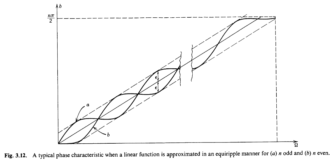
Figure 3 - Equiripple Error Filter Phase Response [2]
For our design we will choose the 0.05 degree phase error equiripple filter from the Handbook of Filter Synthesis [2] textbook (this textbook has plenty of catalogued filters to choose from).
The attenuation characteristics and group delay characteristics of this type of filter can be seen in Curve 13 and 14, respectively. By inspection of the attenuation characteristic curve (Curve 13), we find a 5th order filter will satisfy the requirement that at 200 MHz (4 times cutoff) it will be attenuated by 40 dB minimum. From the group delay characteristic curve (Curve 14), we find the 5th order filter group delay is constant up to around 1.6 times the cutoff so the passband (0 to 1 rad/s because the filter is normalized) will have constant group delay.
With a filter type and order determined that satisfies the group delay and attenuation requirements we can now choose the filter elements based on our \(R_S/R_L\) ratio. The list of LPF prototype element values are presented with different normalized source resistances. To know which one to pick we will normalize our final source resistance by the load resistance. The normalized source resistance is then \(R_{S_{n}} = 25/250 = 0.1\). Therefore, we will choose the element values in the row where \(R_S\) is 0.1 and n is 5 (5th order).

Figure 4 - 5th Order Equiripple Error Normalized Filter
We can now scale the normalized element value with the two steps described above.
-
Multiplying the normalized source and load resistors by the final load resistance. For this example, we would multiply both terminating resistors by 250 ohms.
-
Calculate the final capacitor and inductance values using:
$$ C = \frac{C_n}{2{\pi}f_cR} $$
$$ L = \frac{RL_n}{2{\pi}f_c} $$
After scaling the filter elements we are finished with our design.

Figure 5 - 5th Order Equiripple Error Scaled Filter
We can double check our filter behaves as desired through simulation. In reality, the attenuation and group delay characteristics won't be perfectly matched to the normalized filter because real components have losses and parasitics which alter the filter response.
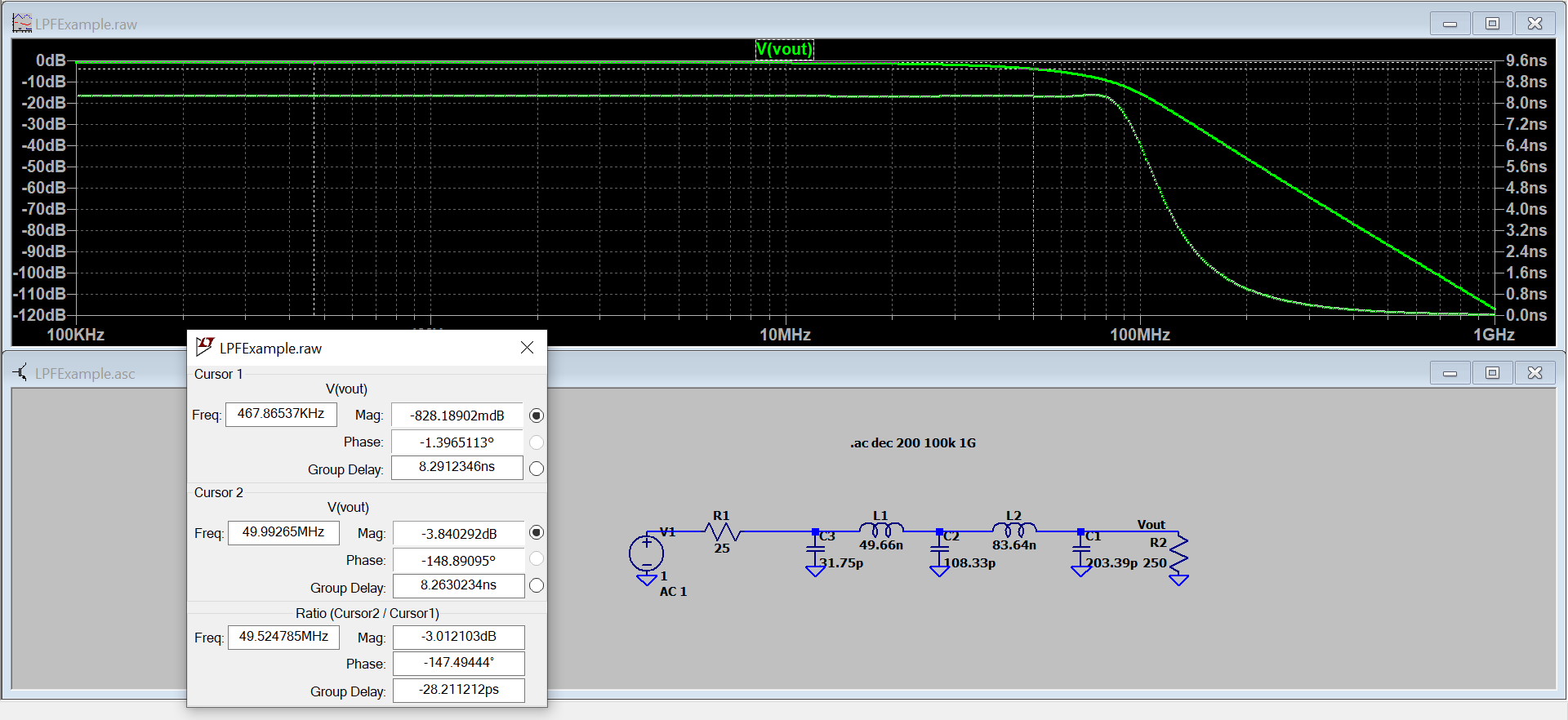
Figure 6 - Attenuation and Group Delay Response of 5th Order Equiripple Error Filter
High-Pass Filter Example
Problem: Design a HPF with a maximum ripple of 0.2 dB, a cutoff frequency at 25 MHz, a source resistance of 100 ohms and a load resistance of 50 ohms. Assume a minimum attenuation of 60 dB is required at 5 MHz.
For our design, we will use the 0.1 dB ripple Chebychev response. To determine the order needed we will look at the normalized attenuation characteristics chart as shown in Figure 3-16 of RF Circuit Design. By inspection, the 4th order filter satisfies the attenuation requirement.
We can now determine the filter element values from Table 3-5A. Our normalized source resistance is \(R_{S_{n}} = 100/20 = 2.0\), therefore we will choose the element values from row \(R_S/R_L = 2.0\).

Figure 7 - 4th Order 0.1-dB Chebyshev Normalized LPF
The filter chosen is a normalized LPF so we must tranasform it into a HPF by replacing each filter element with the opposite type and reciprocal value. Now we can scale each element in the same manner as the LPF.

Figure 8 - 4th Order 0.1-dB Chebyshev Scaled HPF
Again, we can double check our filter behaves as desired through a simulation.
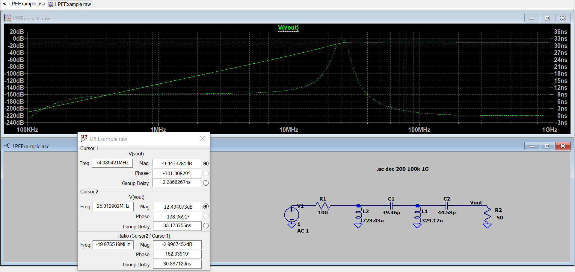
Figure 9 - Attenuation and Group Delay Response of 4th Order 0.1-dB Chebyshev HPF
Bandpass Filter Example
Problem: Design a BPF with a lower 3-dB cutoff at 100 kHz and an upper 3-dB cutoff at 1 MHz. Ensure a minimum of 40 dB attenuation at 3 MHz. Assume a source resistance of 50 ohms and a load resistance of 50 ohms.
The first step when designing a BPF is to convert our requirements into the ratio of bandwidths so that we can choose the appropriate filter response. We can calculate the 3-dB bandwidth as follows.
$$ BW_{3dB} = 1 MHz - 100 kHz = 900 kHz $$
The geometric center frequency, \(f_o\), is therefore,
$$ f_o = \sqrt{(f_{lower3dB})(f_{upper3dB})} = \sqrt{(100kHz)(1MHz)} = 316.23 kHz $$
With the center frequency and the upper 40 dB cutoff, we can compute the lower 40 dB cutoff.
$$ f_{lower40dB} = \frac{{f_o}^2}{f{upper40dB}} = \frac{{316.23kHz}^2}{3MHz} = 33.33 kHz $$
Now we have all the necessary values to calculate our ratios of bandwidths.
$$ \frac{BW_{40dB}}{BW_{3dB}} = \frac{3 MHz - 33.33 kHz}{900 kHz} = 3.3 $$
We can now look through our catalogue to find a filter with 40 dB of attenuation minimum at \(f/f_c\) = 3.3.
For this design, we'll use a Butterworth filter and by inspection of the attenuation characteristic curve (Figure 3-9), a 5th order filter satisfies the 40 dB requirement at \(f/f_c\) = 3.3. Knowing we have equal terminating resistors we can choose the 5th order Butterworth element values from Table 3-1.

Figure 10 - 5th Order Butterworth Normalized LPF
Now we transform the LPF prototype to the BPF configuration.

Figure 11 - Transformed 5th Order Butterworth Normalized BPF
Then scale the element values with the two steps described above.

Figure 12 - 5th Order Butterworth BPF
Finally, we can simulate our filter to ensure it behaves as expected. We find the upper cutoff is a little lower than 1 MHz so if needed we could redesign the filter with a slightly higher upper cutoff frequency.
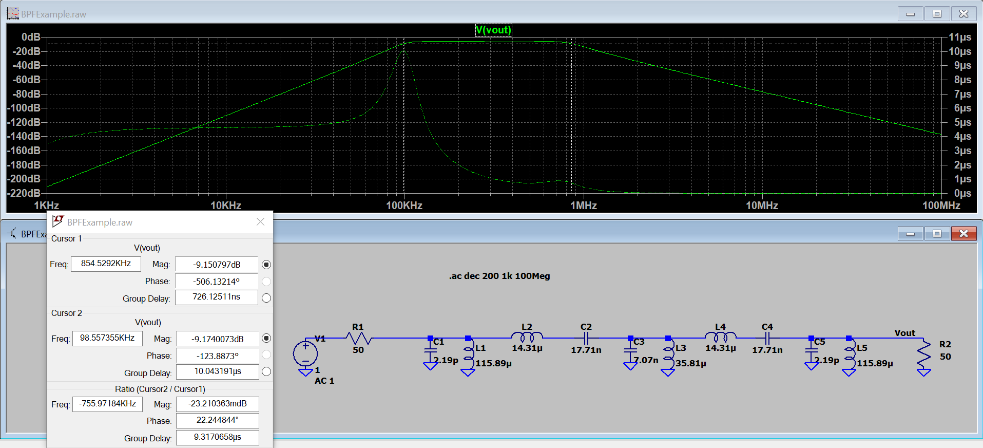
Figure 13 - Attenuation and Group Delay Response of 5th Order Butterworth BPF
References
[1] Chris Bowick, RF Circuit Design, Second Edition, 2008, https://ia801604.us.archive. org/21/items/RFCircuitDesign2ndEdition/RF%20Circuit%20Design%20-%202nd%20Edition.pdf
[2] Anatol I. Zverev, Handbook of Filter Synthesis, 1967, https://ia803101.us.archive. org/20/items/HandbookOfFilterSynthesis/Handbook%20of%20Filter%20Synthesis.pdf