Overview:
- Design of a FMCW radar PCB to be used for range detection and synthetic aperture radar.
- Reasoning for radar hardware design decisions.
- Simulation for receiver signal chain and PCB traces.
Table of Contents
- Introduction
- Initial Steps
- Hardware Design
- PCB Design
- Future Work
- Mistakes and Lessons Learned
- Conclusion
Introduction
This project started as a desire to learn about radar design and synthetic aperture radars. While there are plenty of textbooks that expound on a variety of radar topics, there are few that discuss the steps in designing a system and the engineering trade-offs that need to be made throughout the design process. The curiosity of radar design led me to the work of Henrik's Blog, who designed a functioning Frequency-Modulated Continuous-Wave (FMCW) radar capable of synthetic aperture radar imaging. As soon as I read through Henrik's blog post, I knew that was just the project I wanted to work on.
To further both my hardware and software design skills, I decided building my own FMCW radar from scratch would be a more advantageous project than simply using Henrik's hardware design and software. While it may be trite to begin a project that's already been done, I still knew creating my own FMCW radar would be a great way to bolster my hardware design skill, improve my understanding of imaging radars and gain some valuable troubleshooting experience that can only be learned through overcoming blunders.
I would also like to preface my design with slight caution that there surely will be some errors in my analysis and engineering choices. This entire project is a way to learn, make mistakes and learn from those mistakes so please be wary as the decisions taken for this project are just one of many and may not be the correct or optimal decisions.
There are also many other projects like this elsewhere on the internet, either novel designs, derived from Henrik's project or based off the MIT coffee can radar which provide alternative designs that are worth looking into.
Initial Steps
Decision for Type of Radar
Since I was beginning this project from the very beginning, I set out three general requirements I wanted the radar project to fulfill.
The first requirement was that the system should be functional with relatively close targets (between 3 m to 150 m). This stipulation stems from wanting the ability to test the radar system at a park or soccer field and not some gigantic open field. This seemingly simple requirements meant a few radar design choices would not be tenable. Two main design choices I decided to abandon in response to this requirement was the use of a single antenna for both transmitting and receiving as well as using a pulsed radar waveform.
In a traditional pulsed radar system with a single antenna, the receiver is often blanked (receiver is turned off) when the radar is transmitting to avoid the transmitted signal from overpowering the sensitive receiver. However, this need to wait for the pulse to finish transmitting before being able to detect the reflected echo sets a relatively large minimum detection distance. For example, a pulse width, \(\tau\), of 1 \(\mu s\), which would be the shortest pulse width achievable while keeping component costs reasonable, and a receiver recovery time of 200ns (time to stop blanking receiver and switch antenna to receiver) would result in a minimum range [2] of:
$$ R_{min} = \frac{c\cdot(\tau + 200{ ns})}{2} = \frac{3\cdot10^8\cdot(1000{ ns} + 200{ ns})}{2} = 180 \ m $$
The division by two in the equation above is to account for the signal travelling to the target then reflecting back. So designing a single antenna pulsed radar system would not fulfill my goals to test the radar at close range. However, Henrik was able to design a pulsed compression radar to detect close target but the designed uses two antennas for close distance measurements.
The second requirement was to have a range resolution of around 1 m or less. A system's range resolution is its ability to distinguish between closely-spaced targets. In a single frequency pulsed radar system, the range resolution is determined by the pulse width. For example, a pulse width, \(\tau\), of 1 \(\mu s\) will have a minimum range resolution of:
$$ Range \ Resolution = \frac{c\cdot\tau}{2} = \frac{3\cdot10^8\cdot 1u}{2} = 150 \ m $$
To achieve a 1 m range resolution with a single frequency pulsed radar system, the pulse width would need to be 7 ns wide which just isn't economical for this design. A small pulse width, when the Pulse Repetition Frequency (PRF) and peak power is kept constant, can also diminish the maximum detection range because it reduces the total amount of energy transmitted by the system.
The solution to the dilemma of maximizing both detection range and range resolution is pulse compression. Pulse compression is a technique in which long pulses are modulated followed by “compression” of the received echoes by decoding their modulation [3]. This technique allows the range resolution to be independent of pulse width and instead inversely proportional to bandwidth for frequency modulated pulses or inversely proportional to the number of subpulses in phase modulation. Linear Frequency Modulated (LFM) chirps (another name for pulses) are the most common pulse compression technique, but it requires a wide bandwidth Digital to Analog Converter (DAC) and Analog to Digital Converter (ADC) to obtain the fine range resolution desired, which can be costly.
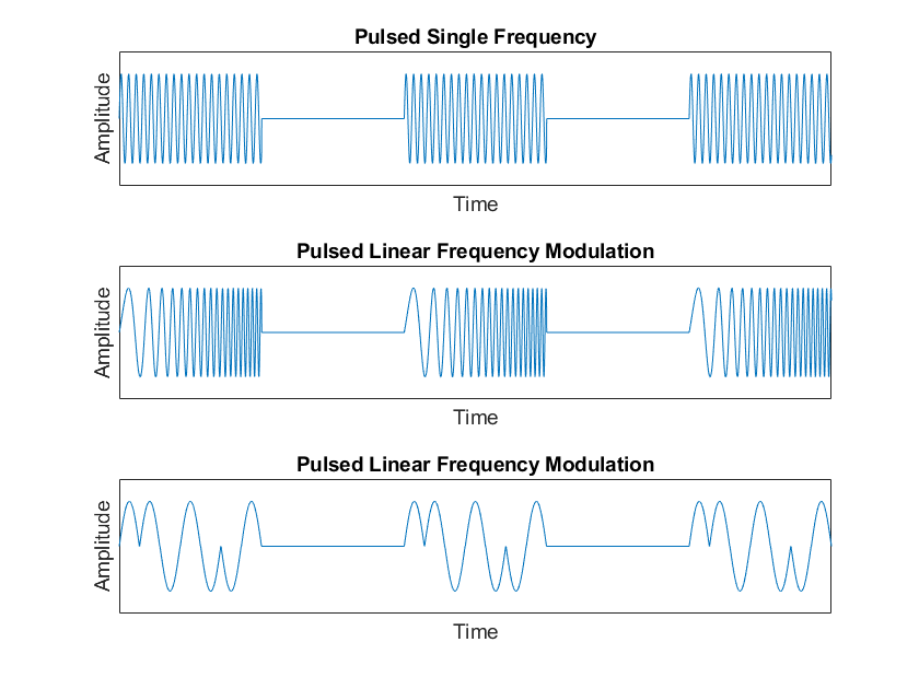
Figure 1 - Pulsed Radar Waveforms
The simplest method for realizing fine range resolution at close ranges is a FMCW system. Range resolution in a FMCW radar is inversely proportional to bandwidth, but in a FMCW design, the transmitter design is less complex and the receiver does not require a wide bandwidth ADC. With the first two requirements clearly favoring a FMCW radar system, it was now obvious the system would be based on a FMCW design.
The third requirement was to have a design that can be used for imaging. In order to create a 2D image, the design needs a high resolution (distance needed to resolve two closely-space object) in both down range (across-track) and azimuth (along-track) dimensions.
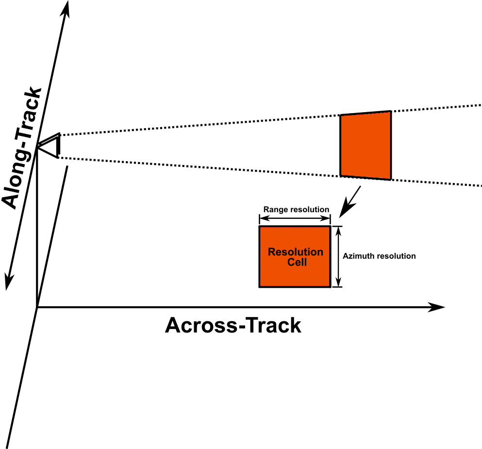
Figure 2 - Radar Resolution Cell
With a FMCW radar system, the range resolution can be made fine relatively easily by using a large chirp bandwidth but it is much more difficult to improve the cross range resolution. Cross range resolution is determined by the width of the antenna beam which can be improved by either operating at higher frequencies or by using a larger antenna [3]. This is because an antenna or antenna array beamwidth is proportional to wavelength (if antenna size is kept constant) and is inversely proportional to aperture/array length or diameter. For example, if a directional antenna with a beamwidth of 30 degrees is used then at a range, \(R\), of 20 meters, the azimuth (cross-range) resolution would be 10.5 m.
$$ Azimuth \ Resolution = R\cdot\theta_{beamwidth} = 20\cdot\frac{30\cdot\pi}{180} = 10.5 \ m $$
This resolution would not be sufficient for any imaging system so one method to increase the cross-range resolution is using Synthetic Aperture Radar (SAR) processing. The basic idea of SAR imaging is to take radar measurements at known increments in a straight track which can then be used together to attain much greater cross-range resolution. By combining multiple measurement, a long virtual or synthetic aperture can be formed, and hence the name Synthetic Aperture Radar. To ensure the FMCW radar system is capable of SAR processing, the design must be capable of transmitting an identical waveform for each consecutive sweep that can be constructively added without any timing or phase differences. After SAR procession, the fine azimuth and down range resolution can be used to represent the data as a 2D image.
FMCW Basics
With it now patent that a FMCW radar system fulfills my three general requirements at the lowest cost, some background on how a FMCW radar works can be provided.
In the simplest form, the radar transmits a continuous signal whose frequency linearly increases or decreases and the instantaneous difference between the frequency of the received echo and the frequency of the transmitted signal is measured which is then converted to a target's range. The basic block diagram consists of an oscillator, OSC, that generates the Frequency Modulated (FM) signal. Common signals are linear sawtooth FM signals, linear triangular FM signals and segmented linear FM signals (this signal can help with resolving ambiguity from doppler shifts).
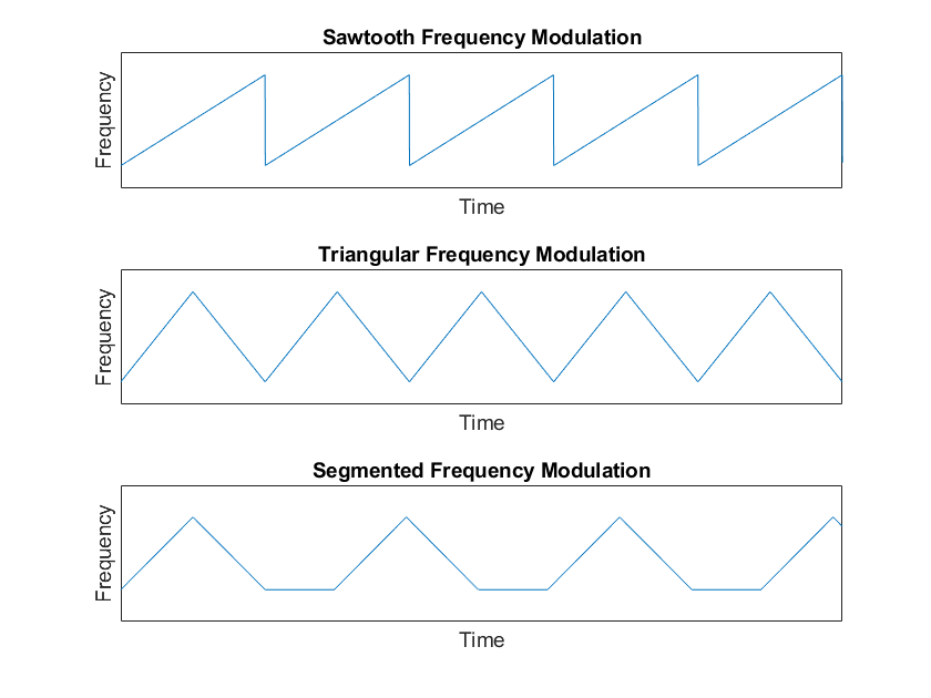
Figure 3 - Frequency Modulated Waveforms
After the oscillator, there is often a power amplifier (PA) to boost the signal power for transmission. The amplified signal is then fed into a splitter or coupler where a portion of the signal is fed into the local oscillator (LO) port of the mixer (MIX) while the remaining signal is radiated out of the antenna (ANT1). The signal then propagates through free-space until it scatters off the target and the echo propagates back to the radar. The echo is received by the second antenna (ANT2), which is a delayed copy of the transmitted signal. The feint signal is then amplified by a low noise amplifier (LNA), then fed into the Radio Frequency (RF) port of the mixer. The mixer then outputs the sum and difference of the signal frequencies at the RF and LO ports. The difference frequency is proportional to the target range, and often called the beat frequency. The sum signal, typically in the GHz range, is then filtered by a low pass filter (LPF) and the beat frequency, typically in kHz to MHz range, is amplified by a video amplifier (AMP). The beat frequency is digitized by the ADC and the distance to the target can be ascertained using Fourier analysis. The greater the target's range, the greater the beat frequency and when multiple targets are present, there will be multiple beat frequencies superimposed on each other at the video output [4].

Figure 4 - FMCW Block Diagram
Another approach to understanding the relation between the difference frequency (beat frequency) and target range is to recognize that the difference frequency equals the rate of change of the transmitted frequency (hertz/second) times the two-way propagation delay. Therefore, the difference frequency can be divided by the frequency rate, often called the chirp rate, to provide the two-way propagation delay and hence the range [3]. For example a 20 kHz beat frequency with a chirp rate of 10 kHz/\(\mu s\) results in a two-way propagation delay of 2 \(\mu s\) which equals a target range of 300 m.
Two drawbacks with this near DC beat frequency architecture is flicker noise in active components that is proportional to the inverse of frequency (1/f) and strong DC offset components so for future designs a low-IF receiver may be worth investigating.
Hardware Design
In the following sections, I'll discuss the design and development of the different sections in the FMCW radar design. The transmitter sections will be discussed first followed by the receiver sections. For each section, I'll expand on the design decisions that were made and the reasoning behind them.
Transmitter
Waveform Generator
Before deciding how to generate the FMCW radar signal, I first had to decide what frequencies to use. To legally transmit the radar signals, I knew I had to stay within the amateur frequency bands such as 2300 MHz to 2450 MHz, 5650 MHz to 5925 MHz, 10 GHz to 10.5 GHz and so on. While there are components for every amateur frequency band out there, there are only a few bands, that due to economies of scale, have dramatically lowered hardware costs. These would include frequency bands like 2.4 GHz used for Wi-Fi standards and Bluetooth or 77 GHz for automotive radar. In addition to cost, the frequency band chosen must have adequate bandwidth to allow for a range resolution of less than 1 m, which means at least a bandwidth of 150 MHz. Typically, the higher frequency bands will have larger bandwidths than their lower frequency band counterparts.
After weighing both cost and bandwidth availability, the 5.8 GHz band was picked. It provides ample access to low-cost components due to use for Wi-Fi standards and the proliferation of sub-6 GHz communication as well as a large enough bandwidth to attain the desired range resolution. The frequency is also not too great therefore inexpensive PCB materials and cables can be used without significant signal attenuation.
There a several ways to generate the FMCW signal, for example we can use a DAC, a Direct Digital Synthesis (DDS) chip, a Voltage Controlled Oscillator (VCO) or a Phase-Locked Loop (PLL).
The DAC and DDS method allows for precise control over the characteristics of the generated signal (phase, amplitude or frequency). The drawbacks are that they often operate in the MHz to low GHz range therefore, they would require an up-converter for the signal to be centered at 5.8 GHz. As well, they often require filtering for harmonics or image frequencies and can sometime require high-speed interfaces to control. For more complex radar systems, DACs or DDS chips would be the preferred signal generation method.
For simpler FM waveform generation, the VCO and PLL can be used. The VCO is an oscillator whose frequency is controlled by an input voltage signal. VCOs can operate from kHz to hundreds of GHz so there would be no need for up-convertion. VCOs are also simple the implement and require little additional hardware. The problem with VCOs is that the frequency ramp-up/down is not perfectly linear and VCOs do not have very stable outputs so the transmitted signal would not be identical between sweeps which would diminish the system's ability to be used for imaging. The PLL solves some of these issues by employing feedback into the system. A PLL can detect the frequency of the VCO then adjust the VCO input voltage to precisely control the VCO output frequency. This greatly improves the stability and linearity of the frequency sweeps. Due to the lower complexity, a PLL was chosen for the waveform generator section of the design.
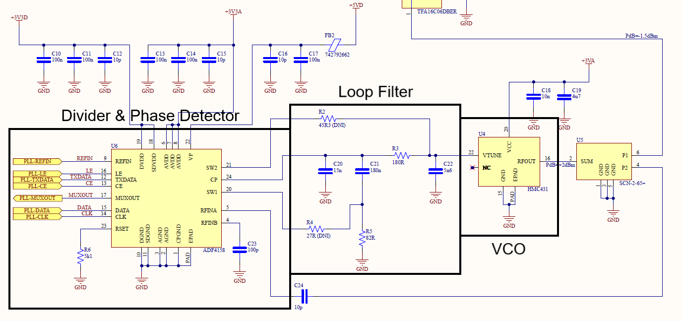
Figure 5 - PLL Schematic
A PLL usually consists of 4 main blocks: a feedback divider, a phase detector, a loop filter and a VCO. For this design, the feedback divider and phase detector sections are performed by the Analog Devices (AD) ADF4158 synthesizer chip, AD HMC431 for the VCO and the loop filter is constructed from discrete components. With the help of the ADIsimPLL software, a suitable loop filter for the type of radar signal expected to be transmitted can be generated and simulated. The loop filter was designed to minimize phase noise and achieve a perfectly linear frequency sweep. These characteristics come at the cost of slow frequency switching, which mean small period and high bandwidth waveforms are not feasible and longer settle time from highest to lowest frequency in sawtooth waveforms. However, the design does not have any restrictions on measurement time and triangle waveforms can be used so the disadvantages were acceptable. Below is the time domain response of the PLL for a triangular frequency modulation waveform.
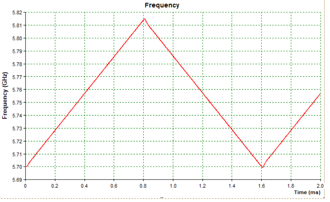
Figure 6 - PLL Time Domain Response
The ADIsimPLL software also provides the expected phase noise of the designed PLL. The phase noise of the transmitted signal sets a lower limit to the ability to resolve closely-spaced targets. Since a FMCW radar system uses low frequency video signals to resolve target distance, phase noise can diminish the system's capability to resolve closely spaced targets. This problem can be exacerbated if the chirp rate is low causing closely-spaced target beat freqeuncies to be even closer together. Phase noise can also create inaccurate readings for both range and velocity and worsen clutter suppression techniques when trying to differentiate between moving and stationary targets.
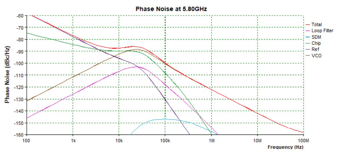
Figure 7 - PLL Phase Noise
Power Amplifier
The next stage after the PLL is the power amplifier (PA) section. Before the waveform is fed into the amplifier, the signal first goes through a 6 dB attenuator to lower the signal power to avoid saturating the output amplifier then passes through a bandpass filter, DEA165550BT-2230C2-H, to remove the harmonics from the VCO output. The filtered signal is then fed into Qorvo RFPA5542TR13. The PA has a rated gain of 33 dB which amplifies the signal to roughly 25 dBm. Both the input and output are matched the 50 ohms so matching networks were not required.
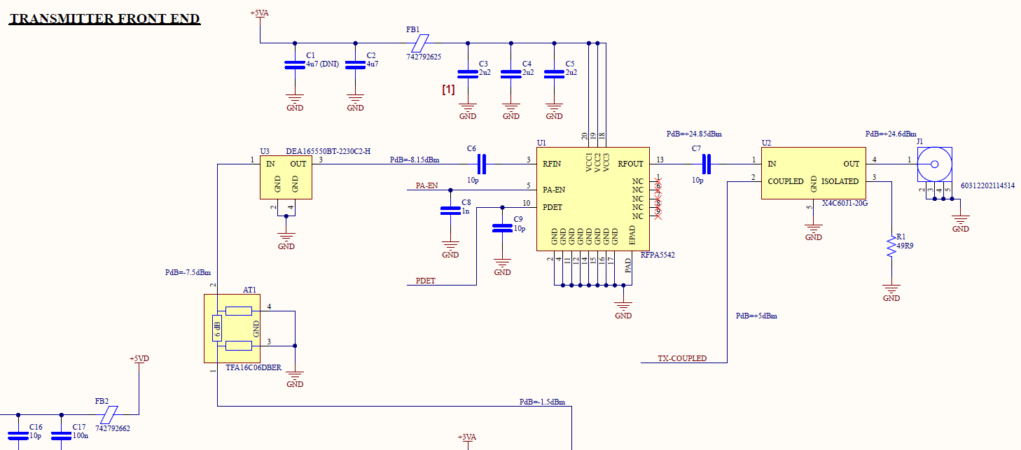
Figure 8 - Power Amplifier and Directional Coupler Schematic
When selecting the PA, I was mainly looking for a single integrated circuit (IC) and that was matched to 50 ohms at both the input and output. With a two-stage amplifier, the design could possibly reach a higher output power but it would come at the cost of a slightly more complex design. The desire for 50 ohms input and outputs also stem from the desire to keep the design simple. Without an Electronic Design Automation (EDA) software like Keysight ADS or Cadence Microwave Office, it can be difficult to model and design matching network for non impedance matched components. The final two features I was designing for was to ensure there is sufficient margin, at least 5 dB, from the output 1 dB compression point (OP1dB) and that the output return loss is greater than 10 dB to avoid reflections from an imperfect antenna. The RFPA5542TR13 has an OP1dB of 33 dBm so we have a 8 dB margin and the PA IC has an input and output return loss of 12 dB which satisfies the characteristics I was looking for.
Directional Coupler
The final section of the transmitter is the direction coupler. This section provides the mixer with a sample of the transmitted signal so the beat frequency can be found. The reason for choosing a directional coupler instead of a power splitter is that with a power splitter, the local oscillator (LO) signal the feeds into the mixer would need to be heavily attenuated to ensure the signal abides by the mixer's LO input power rating. This would be very inefficient, especially when the signal was just amplified in the previous block. As well, a directional coupler provides excellent isolation to the LO port from any signals received from the transmitter antenna as well as isolate any reflections caused by the mixer LO port from the transmitter section.
The directional coupler can be constructed through microstrip transmission lines, like the one made in Henrik's design, but the ability to make the PCB smaller with a discrete component and to forgo simulating the coupler outweighs the cost savings of a single component.
Receiver
Low Noise Amplifiers and Filtering
After the echo is received, the first section the signal will be fed into is the LNA section. The main goal of this section is to create a sensitive (ability to detect small signals) and selective (ability to reject unwanted signals) receiver front end. One key characteristic for outlining the selectivity of your receiver is its noise figure, F, which is the ratio of the signal-to-noise ratio (SNR) of the input signal to the output signal of the receiver.
$$ F = \frac{SNR_{in}}{SNR_{out}} $$
In order to ensure downstream noise sources do not significantly degrade the SNR, we can employ a high gain LNA at the beginning of the receiver signal chain. This concept can be understood by examining Friis's noise figure formula for cascaded amplifiers,
$$ F_{total} = F_1 + \frac{F_2 - 1}{G_1} + \frac{F_3 - 1}{G_1G_2} + \frac{F_4 - 1}{G_1G_2G_3} ... $$
where \(F_{total}\) is the overall noise figure when the first amplifier has gain \(G_1\) and noise figure \(F_1\) , the second amplifier has gain \(G_2\) and noise figure \(F_2\) and so on. We see that if the gain of the first amplifier \(G_1\) is large, the following stage's contribution to the noise figure become negligible. Therefore, if \(G_1\) is larger, the receiver noise figure is largely determined by the noise figure of the first LNA in the receiver signal chain.
However, high gain and low noise LNAs often saturate at fairly low input powers so there is a tradeoff between improving receiver noise figure and improving receiver linearity over a large range of received signal powers.
The LNA chosen for the first amplifier in the receiver chain is Quorvo QPL9504. It has a gain of 21 dB and noise figure of 0.76 dB within the operating bandwidth. However, its OP1dB is 18.7 dBm, meaning we should keep the input power around -8 dBm and below to maintain linearity. Admittedly, the low-noise and high-gain advantages of this particular IC involves additional complexity by way of a few external components for biasing and for matching the input and output ports to 50 ohms. Luckily, there is a reference design for the 5.8 GHz frequency band so the implementation required little work.
I wanted the option to use the radar system for targets farther than 100 m just in case, so I decided to add a second LNA. The second LNA is the Skyworks SKY65981-11, which has a very interesting feature in that the LNA can be bypassed. The gain is only 13 dB typical and has a noise figure of 1.5, but since the first LNA often dictates the system's noise figure the higher noise figure is not an issue. The input 1 dB compression point (IP1dB) is -1.5 dBm typical, but as mentioned earlier, the LNA can be bypassed if we detect the second LNA is near saturation. However, when the LNA is in bypass mode, the LNA has an insertion loss of 7 dB which will significantly degrade the receiver's noise figure. Nonetheless, when bypass mode is needed, the signal strength should be high enough to not be impacted by the added noise.
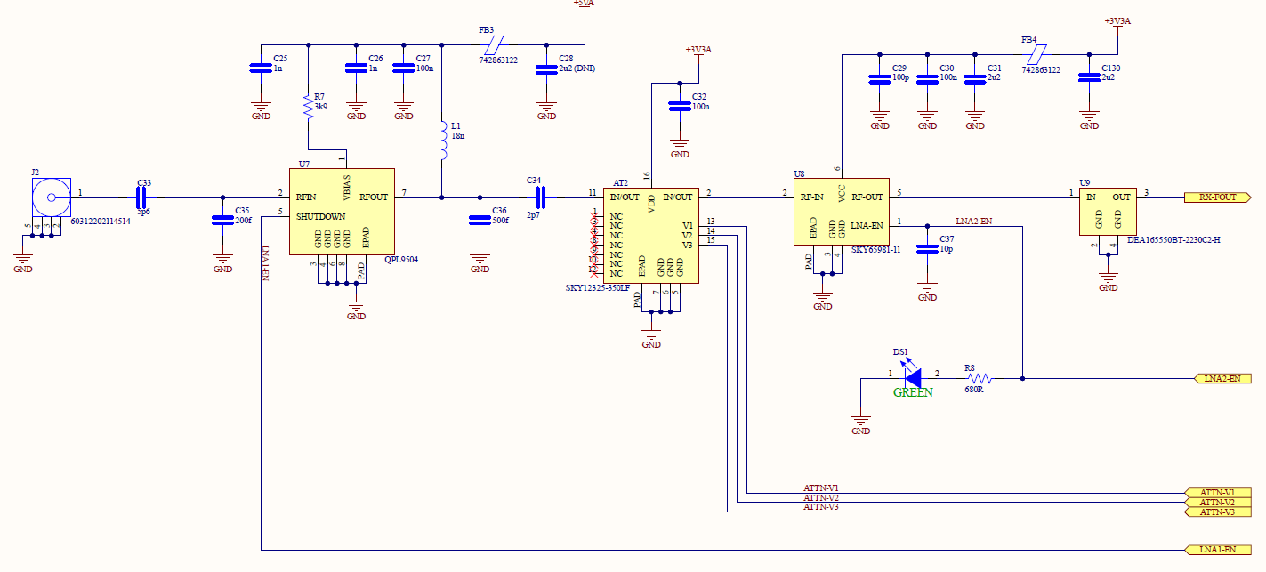
Figure 9 - Receiver Front-End Schematic
The one notable problem with using these two LNAs consecutively is the possibility of reflections due to the poor output return loss of LNA QPL9504, 9.3 dB, and even worse input return loss of LNA SKY65981-11, 7dB. To ameliorate this issue, a variable attenuator with good input/output return loss was added between the two LNAs. A simple fixed attenuator could have been used but the flexibility of a variable attenuator felt more appropriate for this design. While the distance between LNAs would not be an appreciable portion of the signal's wavelength if the variable attenuator was not used, without an EDA or Electromagnetic (EM) simulator to verify there would be no signal integrity issues, I thought it would be safer to add the additional hardware to obviate any future problems.
Finally, a bandpass filter (BPF) was placed after the two LNAs to attenuate out of band signals as well as limit the amount of noise entering the system. The decision to place the BPF after the amplification stage was based on the desire to lower the noise figure. This choice, however, comes at the cost of potential out-of-band noise or third order products saturating the LNAs. I don't expect to be operating in environments with other transmitting devices so I decided to accept this risk, furthermore the ability to adjust the LNA gain using the variable attenuator and bypass the second LNA should limit the severity of this possible issue.
Having the filter closer to the mixer input may, in theory, help limit the amount of the mixer sum product from coupling back onto the receiver signal chain because it will be filtered out by the BPF. The extent of the benefit is probably negligible and is difficult to determine without an EM simulator.
With the front end completed, we can now estimate a few parameters about the radar receiver. The first of which is the maximum received power at the receiver antenna to ensure LNA and mixer linearity. With the second LNA bypassed and the variable attenuator set to its highest value, the loss between the first LNA and the mixer will be around 16 dB. The first LNA has an OP1dB of 18.7 dBm and the mixer has an IP1dB of 11.3 dBm which means the LNA will saturate sooner and therefore is the limiting component that will set the maximum input power. Using a margin of 5 dB from the IP1dB point, the maximum received power will be -8 dBm.
When the second LNA is enabled and the variable attenuator is set to 0 dB, the second LNA becomes the first component to saturate and the receiver power will need to be below -27 dBm to avoid nonlinearities.
What does this signify? Well this can be used to determine our minimum spacing between transmit and receive antennas. Using the Friis transmission formula [5]:
$$ P_{r} = P_{t}\frac{G_tG_r\lambda}{4\pi R}^2 $$
Where:
\(P_r\) = the power at the receiver antenna
\(P_t\) = the power at the transmitter antenna
\(\lambda\) = wavelength
\(G_t\) = transmitter antenna gain in direction of receiver antenna
\(G_r\) = receiver antenna gain in direction of transmitter antenna
\(R\) = distance between antennas
We can determine a safe distance for our antennas to avoid saturation. \(P_t\) will be +25 dBm, \(\lambda\) will be the worst case wavelength at 5.65 GHz (0.053 m), \(G_t\) and \(G_r\) can be found from the antenna datasheet, (will use -10 dB for both), and now we can plot the received power versus separation distance.
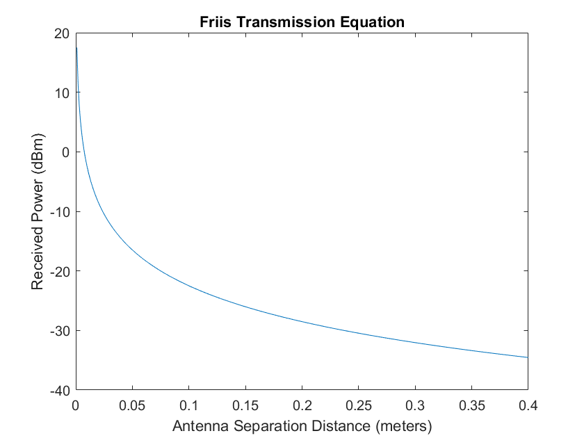
Figure 10 - Antenna Coupling
From this plot we find a separation distance of around 2 cm leads to a received power of -8 dBm. However, the Friis formula above is only valid in the far field so this distance is not exactly accurate. We would like to use the radar when the second LNA is enabled and variable attenuator is set to 0 dB so the separation should be greater than 17 cm to achieve a received power less than -27 dBm. Once assembled, the separation distance will be closer to 30 cm (~1 ft) so there should not be any issues.
Furthermore, the minimum target distance to avoid front end saturation can also be determined using the radar range equation [5]:
$$ P_{r} = P_{t}\frac{G_tG_r{\lambda}^2\sigma}{4\pi^3R^4} $$
Where:
\(P_r\) = the power at the receiver antenna
\(P_t\) = the power at the transmitter antenna
\(\lambda\) = wavelength
\(\sigma\) = radar cross section (RCS)
\(G_t\) = transmitter antenna gain in direction of receiver antenna
\(G_r\) = receiver antenna gain in direction of transmitter antenna
\(R\) = distance between antennas
The radar equation allows us to estimate the power of the received echo from a target with a radar cross section, \(\sigma\). Therefore, we can estimate a minimum distance for linear operation by setting \(P_t\) to +25 dBm, \(\lambda\) set to the center frequency 5.8 GHz (0.052 m) , \(G_t\) and \(G_r\) set to the gain of the main beam (8 dB), \(\sigma\) set to the RCS of a person, \(1 m^2\), and now we can plot the received power versus target distance.
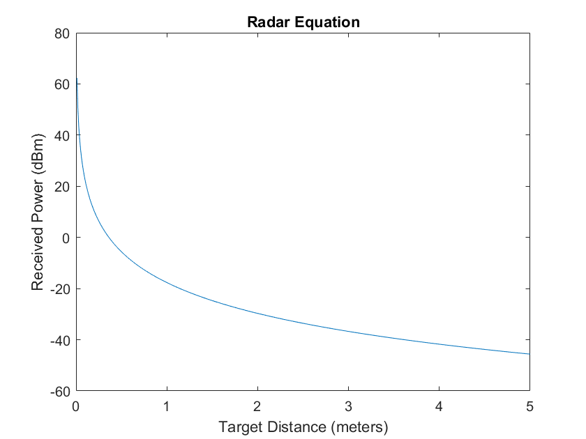
Figure 11 - Radar Equation
Thus, we have determined that we should keep a minimum distance of at least 0.6 m (-8 dBm) from the radar system to avoid saturating the front end when operating with the second LNA bypassed and the maximum variable attenuation.
Mixer
The next section of the receiver chain is the mixer stage. In this section the sample of the transmitted signal is multiplied with the received signal to create the beat frequency. An ideal mixer is a hardware implementation of multiplying two signals. The mixer can be understood by examining the trigonometric identify when two sinusoidal functions are multiplied:
$$ cos(2\pi f_1t)cos(2\pi f_2t) = \frac{1}{2} \cdot [cos(2\pi(f_1 + f_2)t) + cos(2\pi(f_1 - f_2)t)] $$
Which illustrates that when two signals are multiplied together, they create a resulting signal that comprises a sum component, \(cos(2\pi(f_1 + f_2)t)\), and a difference component, \(cos(2\pi(f_1 - f_2)t)\).
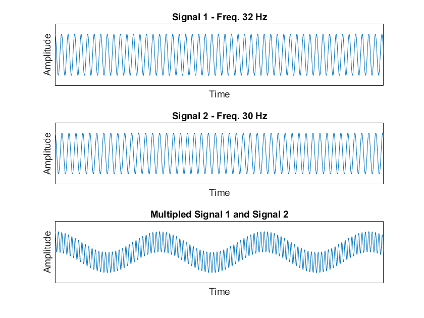
Figure 12 - Signal Mixing
In our FMCW radar system, the mixer will mix the sample of the transmitted signal with the received echo. Because the received echo is essentially a delayed version of the original waveform, the mixed frequencies will output a sum frequency around 10 GHz and a difference frequency in the kHz to MHz range. This difference frequency, often called the beat frequency, is the signal we wish to analyze.
The mixer chosen for this design is the AD ADL5801. This mixer is an active mixer, so it provides around 0 dB of gain but has a high noise figure. Passive mixers introduce less noise into the system but often require higher input powers to function linearly. Using an active mixer allows the design to use a lower power LO and RF signal. This also allows the majority of the PA output power to be delivered to the transmit antenna instead of splitting the power to feed a passive mixer LO port. An active mixer also allows us to down-convert lower power echoes than with a passive mixer. Moreover, the noise figure will be dominated by the LNA noise figures, so I wasn't too concerned with the high noise figure (~16.2 dB) of an active mixer. Lastly, power consumption was not a concern for this design, thus the additional power draw for an active mixer was not an issue.
The mixer design was relatively straight forward and copied from the datasheet, however two features are slightly different from the OEM's design. Between the directional coupler and the LO input, a 3 dB attenuator was added. This lowers the power to the desired level but also helps to mitigate reflections from the non-perfect matching from the balun and LO port. The other feature that should be noted is the intermediate frequency (IF) port biasing. The IF ports need to be biased to around 3.75V and for most designs this is done with some form of inductor that allows the DC biasing without letting the IF signal into the power supply lines. Since our IF is such a low frequency, inductors would not impede the IF signal from entering the power supply lines so resistors are used instead. But this still allows a portion of the IF signal to enter the power rail so large capacitors were added to hopefully bypass the IF signal to ground. This feature was difficult to simulate because in most free software, voltage sources are ideal and do not account for all the parasitics in the supply lines, so they will not show any ripple on the line. Power supply integrity was a noticeable weak point throughout the design due to the inability to simulate the power supply system.
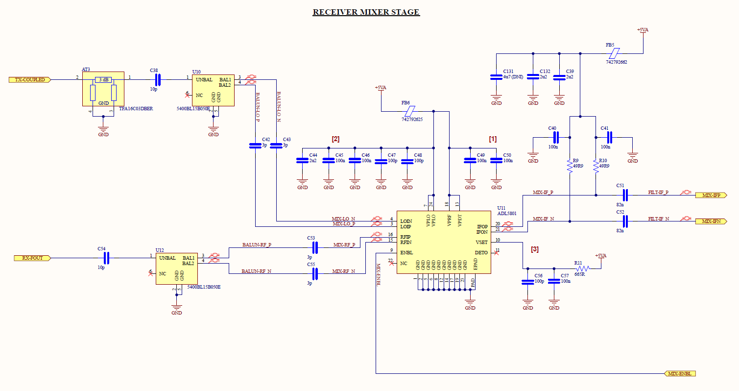
Figure 13 - Mixer Schematic
Video Amplifier and Filtering
Following the mixer stage, is the video amplification and filtering stage. The goal of this stage is to:
- Provide low-pass filtering to remove the mixer sum frequencies and any RF or LO leakage into the IF port.
- Provide high-pass filtering to dampen the higher power echos from close targets.
- Provide amplification to the video signal.
At first, I was planning to use a passive LC filter followed by a differential or single-ended amplifier but the major problem with LC filters at such low frequencies are the very large component values required. The most problematic components are the large inductors that would be needed to synthesize an LC filter with a cutoff frequency in the kHz to low MHz range. The solution to this problem, and what was chosen for this design, is to use an active filter which removes the need for inductors and instead only uses resistors and capacitors as well as manageable capacitor component sizes and values. There are a variety of topologies for active filters but the two designs that were initially investigated due to their ability to be easily synthesized using normalized filter tables were the Sallen-Key topology and Multiple Feedback (MFB) topology. In order to reduce susceptibility to common-mode noise, I wanted the signal to stay differential as long as possible so differential active filters were chosen. Since the MFB topology only uses feedback to one input, the inverting input, the design can more easily be transformed from single ended to differential so the MFB topology was chosen. The optimal topology may not have been chosen for this design so further research is needed into this topic.

Figure 14 - Sallen-Key and MFB Topologies
For greater flexibility, the video/IF section uses two separate active low pass filter sections, one for close targets and another for distant targets. To simplify the filter design, the high-pass filtering will be implemented separately from the active low-pass filters. Using a double pole double throw (DPDT) relay, the microcontroller can switch between the two different filters. Since, I don't expect to be switching between the filters frequently, the latching version of the relay was used so once switched there is no continuous current draw. No large decoupling capacitors were added to the power rail near the relays because the relays will be switched while the system isn't operating so any supply line voltage ripple will not affect performance.
Next the filter response needed to be chosen. Since received power diminishes with the fourth power of target distance, I believed a high-order filter with a steep attenuation curve wasn't necessary because the higher beat frequencies, which corresponds to more distant targets, will inherently be attenuated at -40 dB/decade. There is also minimal concerns about unintentional signals from entering the receiver so high attenuation filtering is not required. Additionally, to keep cost and complexity low, I wanted to avoid high-order filters. Lastly, the MFB topology chosen is equivalent to a second-order active filter with gain so an even order filter response was needed. With these factors in mind, the filter response chosen was a 4th order 0.1-dB ripple Chebyshev response because it provides adequate attenuation steepness, the passband ripple is not an issue and does not possess any sharp variations in the group delay.
With the response chosen, the normalized pole locations, Table 10-23 of [6], can be selected:
$$ -0.2177 \pm j0.9254$$ $$ -0.5257 \pm j0.3833$$
These poles can then be used to find the normalized component values using the following formulas [6]:
$$ C_1 = (A + 1)(1 + \frac{\beta^2}{\alpha^2})$$ $$ C_2 = 1 F $$ $$ R_1 = \frac{\alpha}{A(\alpha^2+\beta^2)}$$ $$ R_2 = \frac{AR_1}{A+1}$$ $$ R_3 = AR_1$$
Where:
\(A\) = filter gain of -A
\(\alpha\) = the real part of the pole
\(\beta\) = the imaginary part of the pole
Finally, the components are denormalized by frequency and impedance scaling as follows:
$$ R^{'} = R\cdot Z $$ $$ C^{'} = \frac{C}{FSF \cdot Z} $$
Where:
\(R, C\) = the normalized component values
\(R^{'}{, }C^{'} \) = the denormalized component values
\(Z\) = the impedance scaling factor
\(FSF\) = the frequency scaling factor
For the close range filter, the gain is set to 2 for each stage (total gain of 4), the FSF set to 70 kHz (the LPF cutoff frequency) and the impedance scaling factor set to 2000. For the far range filter, the gain is set to 4 for each stage (total gain of 16), the FSF set to 300 kHz (the LPF cutoff frequency) and the impedance scaling factor set to 2400.
After scaling the component values, the following active LPFs were designed:
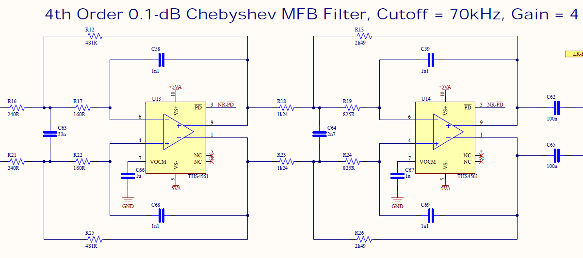
Figure 15 - MFB Close Range Filter Schematic
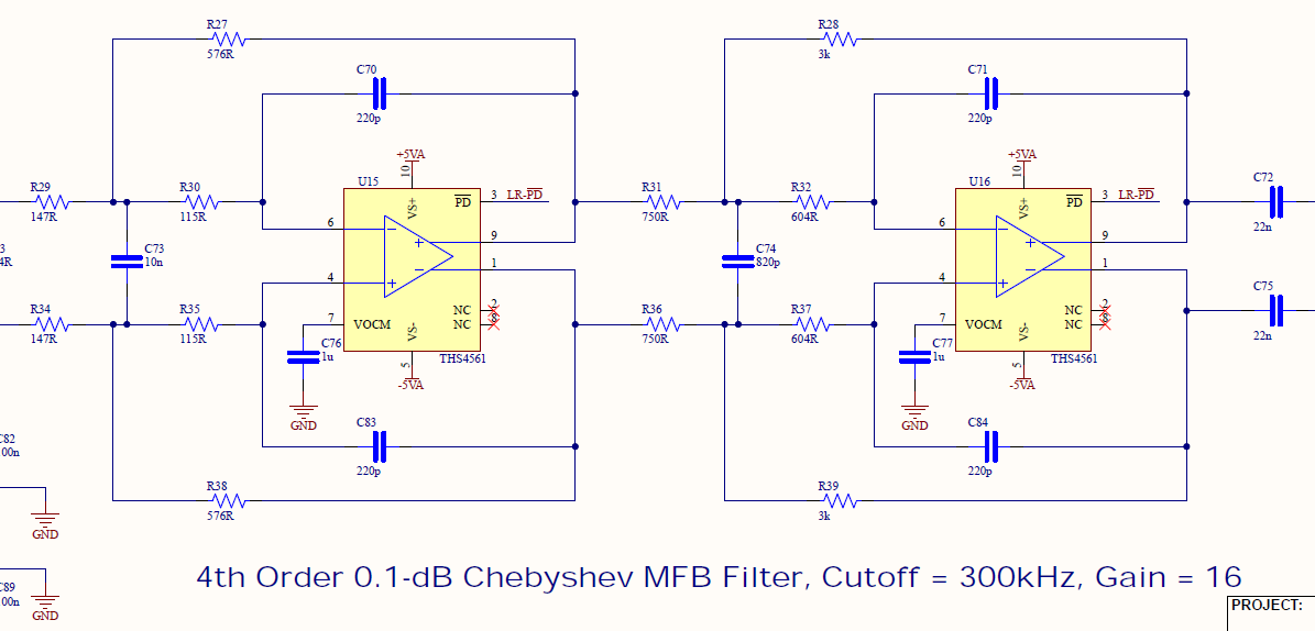
Figure 16 - MFB Far Range Filter Schematic
The frequency scaling factors were calculated to cutoff frequencies above a certain range depending on the filter. Assuming a bandwidth of 150 MHz and a sweep time of 1 ms, we can estimate the beat frequency for a specified range with the following equation:
$$ f_{beat} = \frac{2 \cdot R \cdot BW}{T_s \cdot c}$$
From this equation, we can set the filter cutoff frequency based on the maximum desired range. For a bandwidth of 150 MHz and a sweep time of 1 ms, the cutoff range was set to 70m and 300m for the close range and far range filters, respectively. However, the maximum range will change if the bandwidth or sweep time is altered.
The impedance scaling factor was chosen to minimize the resistor values to decrease thermal noise but sufficiently large to try to match the output impedance of the mixer IF ports.
The gain for the two active filters are different because close range target echos do not need to be amplified as much compared to distant target echos. So the close range active filter has a lower total gain compared to the far range filter. The gain chosen also had to ensure there was sufficient bandwidth for the filter so low gain-bandwidth product differential amplifiers could not be used. Finally, the exact gain chosen for each active filter was adjusted after simulating the entire video amplification and filtering section and adjusted accordingly to establish a relatively flat ADC input voltage that is independent on target range.
For the high-pass filtering, two RC high-pass filters were used to offset the -40 dB/decade loss in signal power. The first RC filter was realized in conjunction with the mixer IF port DC blocking capacitors that are needed to prevent the DC bias voltage from entering the filters. The second RC filter was placed after the active filters. The cutoff frequencies were adjusted through testing.
The final stage before the ADC is the differential to single ended converter. This function is performed by the instrumentation amplifier TI INA849. The main reason for this component was to add some additional gain to the receiver that can be adjusted if needed (through a single external resistor). While most advanced ADCs use differential inputs, the ADC used in this design can operate with single ended or differential inputs without any serious degradation in performance so single ended was chosen. The ADC also recommends a transformer coupled input for differential driven inputs but due to the extremely low IF frequencies, finding a suitable transformer would be difficult.
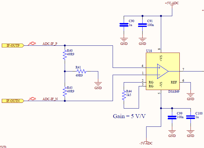
Figure 17 - Instrumentation Amplifier Schematic
With the entire video filtering and amplification section complete, it could now be simulated to ensure performance is as expected. LTSpice was used to simulate the response of the video amplifiers and filters while Matlab was used to compute the voltage at the mixer's IF port and calculate the voltage at the ADC input for target distance.
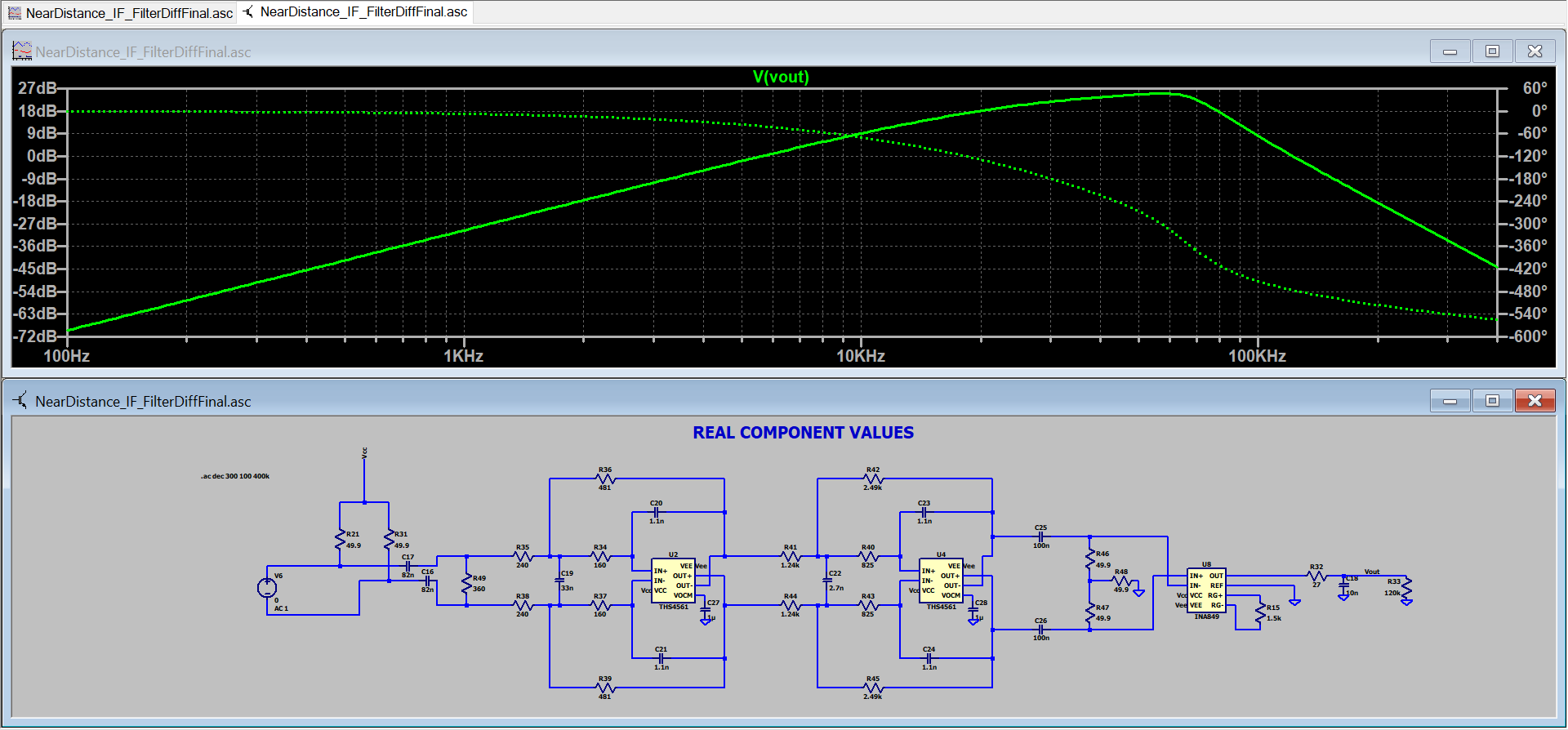
Figure 18 - Close Range Filter Response
The entire simulation consists of the following steps:
- Complete an AC analysis of the designed video amplification and filtering circuit in LTSpice.
- Save the results to a text file.
- Convert the frequency data from the text file into target range using the beat frequency formula. This was done so the AC analysis magnitude aligned with received power.
- Calculate the received power for the list of target ranges found in step 3 using the radar equation.
- Add and subtract any gains or losses in the receiver signal chain.
- Convert the calculated power to voltage at the mixer IF port using the equation \(V = \sqrt{P*R}\).
- Multiply the voltage at the IF port by the gain from the AC analysis in the text file.
- The result will be the expected voltage at the ADC input versus target range.
This may not be the correct method but these were the steps taken to verify the amount of gain and cutoff frequencies for the filters as well as the method used to verify the ADC input was within its input range for all target distances.
Below are the expected ADC input voltages for a sweep bandwidth of 100 MHz and 200 MHz, sweep time of 1 ms, and using the close range active filter.
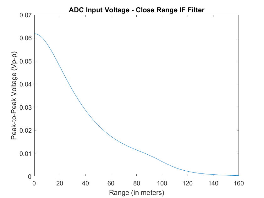
Figure 19 - Simulated ADC Input (100 MHz bandwidth, 1 ms sweep)
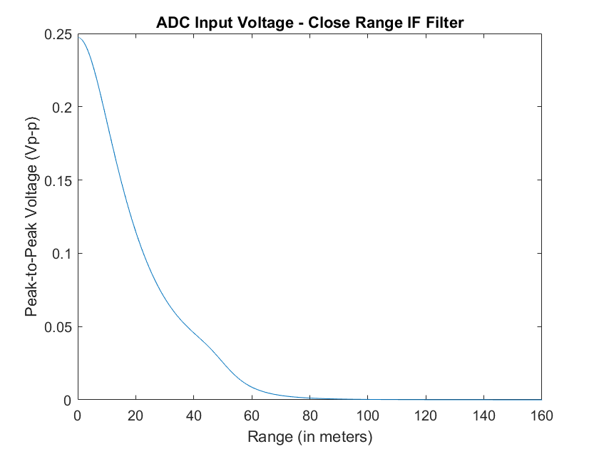
Figure 20 - Simulated ADC Input (200 MHz bandwidth, 1 ms sweep)
All analysis was done without any component tolerances that could change the characteristics of the active filter, so a Monte Carlo simulation to observe performance variation would be another aspect to further investigate. As well, the received power formula does not include any noise or accurately simulate the expected output signal, so it would be beneficial to simulate the entire system in a software such as Keysight PathWave or Microwave Office VSS if the software was avaiable.
Another approach to the video amplification and filtering stage is using automatic gain control (AGC) to vary the gain of the IF stage to increase and decrease the gain of the amplifiers depending on the signal's power or voltage. The IF stage can also just amplify the signal without filtering then get sampled by the ADC. The filtering is then accomplished digitally, instead of using analog filters, which allows for greater flexibility and acquires all information received. This approach is the normal trend of most RF systems because of the ability to filter the signal digitally and moving the ADC as close as possible to the antenna. However, without a foundation in digital signal processing (DSP) and working with FPGAs, I didn't want to complicate the design further as it would take much longer to implement.
Lastly, the power down control signals for the four fully differential amplifiers are fed through a voltage level shifter, TI TXB0108, so they can be controlled by the MCU's 3.3 V logic.
Analog to Digital Converter
In this section the ADC converts the analog continuous-time signal into a digital discrete-time signal. Since FMCW radar system output a low frequency video signal at the mixer's IF port, a high-speed ADC is not required thus, we can minimize cost. The ADC chosen is the 12-bit 10 MHz AD LTC1420IGN. Instead of spending more for a higher bit ADC, it was cheaper to instead over-sample the signal to improve SNR. For example, if the ADC samples at 10 MHz then is digitally filtered at 500 kHz, the resulting oversampling ratio is 10 and this should result in a 10 dB increase in the ADC SNR.
Full analysis of the ADC noise floor and the input noise is needed and will be added in the future.
The analog filtering preceding the ADC helps to remove signals above the Nyquist frequency from folding into the first Nyquist zone (DC to sample rate divided by two, \(F_s/2\)). Without the IF filtering, sometimes called an anti-aliasing filter, signals from other Nyquist zones would appear as targets in our digitized signal.
The 10 MHz 12-bit ADC will create a stream of data 120 Mbps which will be passed to the USB Hi-Speed (HS) interface. USB HS has a maximum data rate of 480 Mbps and using the microcontroller Direct Memory Access (DMA) feature, the microcontroller should be able to transfer the ADC data directly to USB interface without having to store excessive amounts of data. Having the ADC data transferred to the USB HS transceiver through the MCU also allows the MCU to store and process any data if needed in the future
To allow the ADC to communicate with the MCU, voltage level shifters, TI TXB0108, were added to convert the ADC 5 V digital input/output to 3.3 V for the MCU.
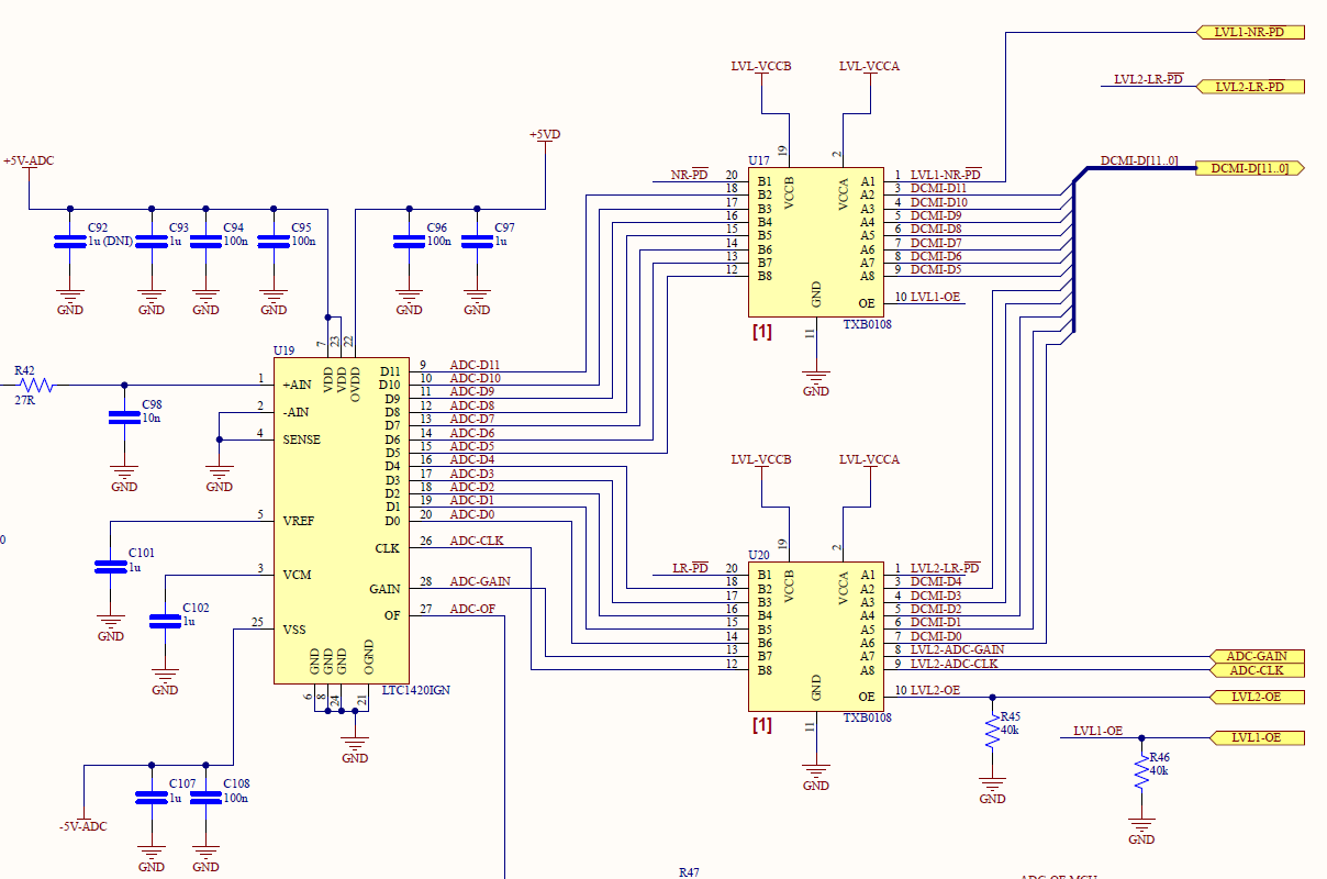
Figure 21 - ADC Schematic
Digital Section
USB Input/Output
After digitizing the target echos, we now need to process them to transform them into useful information such as target distance, target velocity, etc. This can be accomplished using field-programmable gate array (FPGA) ICs to filter and process the radar signals directly on the PCB. However, without much experience with FPGAs and DSP algorithms, it was simpler to transfer the data directly to a PC where the algortihtms could be implemented in Python and visualized on the monitor of a laptop. In order to carry out this method, we need to transfer all the stream of ADC data to the PC which is approximately 120 Mbps.
Most microcontrollers have USB full-speed transceivers built directly into the IC which support a data rate up to 12 Mbps. However, this would inhibit direct transfer from the ADC to PC and data would instead need to be stored or else the information would be lost. Due to the considerable amount of data the ADC outputs it would need to be stored external to the MCU and would require additional hardware and complexity.
Rather than storing the data, a USB HS transceiver Microchip USB3317 was used to substantially increase the data rate to 480 Mbps maximum. This should allow data to be transferred directly to the PC where memory is widely available and does not require additional cost or complexity to integrate.
One additional design note is that the USB cable shield is connected directly to the PCB ground. Ideally the shield would be connected to the enclosure so noise coupled onto the exterior of the shield would not be fed directly onto the ground plane. But if the shield is not connected to ground at both ends, the shield will act as an antenna which causes different issues. We are also not worried about low frequency current returns from flowing on the shield so shielding at both ends should not cause significant issues.
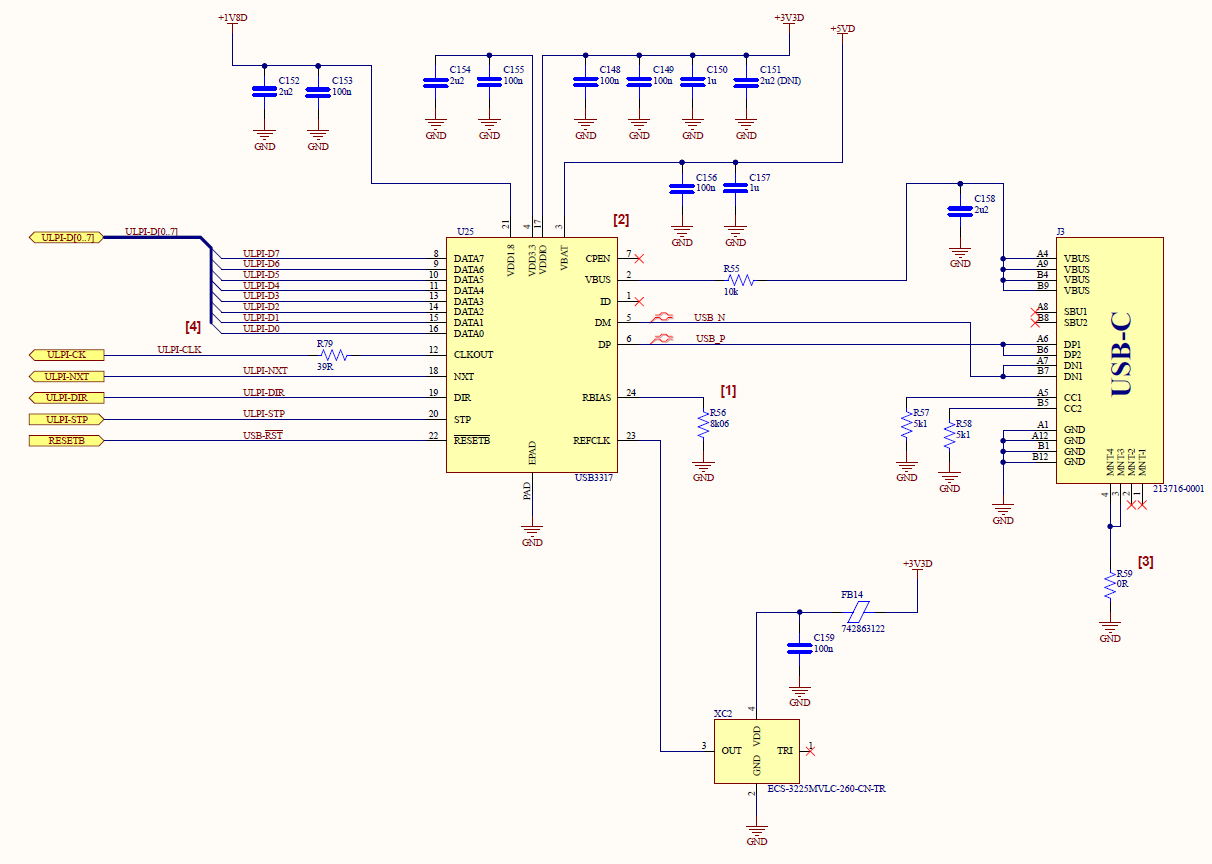
Figure 22 - USB HS PHY Schematic
Microcontroller
In order to operate the transmitter and receiver sections of the FMCW radar, we need some programmable IC that can control and interface with all the components. For this design, the STM32 STM32F429VET6TR microcontroller (MCU) was chosen to fulfill this task.
The process to determine which MCU to use first required to identify the necessary communication interfaces and the number of general purpose input/output (GPIO) pins required for the design. For example, the PLL IC requires an SPI interface and several GPIO pins to operate while the variable attenuator only requires 3 GPIO pins to control the IC. After outlining all the necessary interfaces and GPIO pins needed to interact with all components, we needed to determine other characteristics needed to satisfy the design such as available memory and minimum operating frequency. Since we don't plan to store any data on the MCU other than the program data and program variables, there were no real prerequisites for the amount of memory required. On the other hand, in order to transfer the ADC data to the USB transceiver without inhibiting the ADC sampling rate, the operating frequency of the MCU has to be sufficiently high to forward the incoming ADC data to the USB ULPI interface.
The STM STM32F429VET6TR was able to satisfy all these requirements with some margin. The only exception is that this MCU does not have a specific communication interface to read the parallel output of the ADC but fortunately, the Digital Camera Interface (DCMI) can be configured, so it can be used to read the parallel ADC output.
There are several other companies that make MCUs that could meet the requirements of the design, but I am most familiar with the STM ecosystem so that was the brand chosen.
The next step to help visualize if the MCU meets the requirements was to open the MCU in STM32CubeMX and begin assigning pins to necessary communication interfaces. For most MCUs, certain pins are reused for multiple functions so although the datasheet states the MCU has enough interfaces, once the pins are assigned to a single function, the MCU might be lacking some essential functions for your design. With STM32CubeMX, we can assign the pins before purchasing the MCU, so we can ascertain if the MCU is suitable for the design. When assigning pins, the higher importance interfaces were assigned first and generic GPIOs pins were assigned last. This ensures that we do not use unique pins that are needed for certain interfaces as GPIO pins for menial tasks that any pin can do. During the pin assignment process it is also helpful to have an idea of the orientation of the MCU relative to all the other components. This helps with assigning section specific interfaces and GPIO pins close to those sections so easy direct traces can be used.
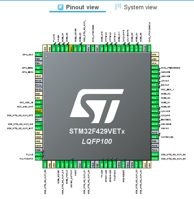
Figure 23 - STM32CubeMX
When assigning pins, most of the assignments were straightforward however, there were a couple aspects worth elaborating on. The first is the clock system, which stems from a single 20 MHz clock. In order to implement proper signal processing, the ADC and PLL needs to be referenced from the same clock so successive sweeps are coherent to each other and to prevent the timing of one IC from drifting away from the other. Since, I wanted some configurability with the sample rate of the ADC, I settled on using the 20 MHz master clock output for the MCU and PLL then using the MCU's main clock output (MCO) to reference the ADC at 10 MHz. While the MCU will add some jitter to the ADC clock, this method allows the design to lower the ADC sample rate if necessary using the MCU MCO divider.
Another aspect about pin assignment worth discussing is to ensure that the MCU's I/O current ratings are followed. For certain high current switching, such as the IF filter relays, external transistors were used to switch the relays since the MCU is not able to provide enough current. Also, with many MCU pins required to source current to toggle pins, it was important to verify the sum of the sourced current does not surpass the MCU limit. Therefore, when possible, GPIO pins, such as the LEDs, were configured to sink current instead of source current to stay within the total sourced/sunk current limits for the I/O pins.
An FPGA is probably more suitable for radar designs because it allows for higher speed interfaces and easier implementation of digital signal processing. Without much experience with FPGAs, I thought it may complicate the design and cause the design and implementation to take significantly longer than with a method I already have experience with. Admittedly, using an FPGA would be the better approach and will be investigated for new version of the design or for future projects.
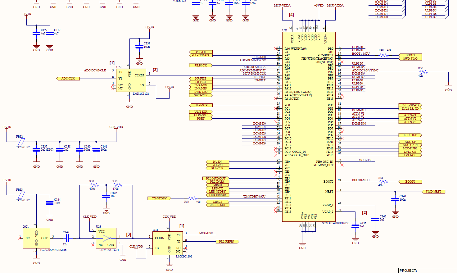
Figure 24 - Microcontroller Schematic
Status and I/O Hardware
Some remaining GPIO pins not used to control the transmitter and receiver sections, were used to add status LEDs, a standby/transmit switch and miscellaneous input/output pins that can be used in the future. The LEDs will help identify different operating modes and any failures and the switch will allow the transmitter to be enabled and disabled externally. In previous projects, I often miss these types of features because they are not necessary but when operating the design they will be extremely useful. The miscellaneous input/output pins do not have any function at the moment but could be used to operate external devices as required.
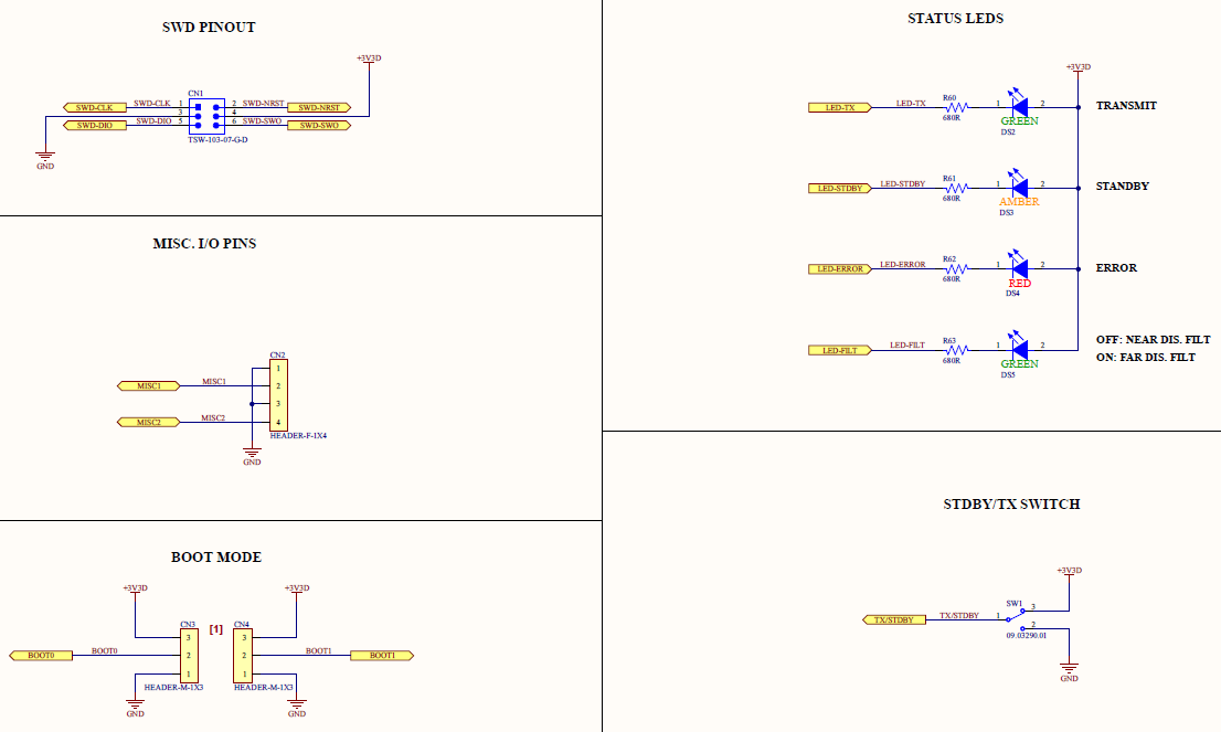
Figure 25 - Status and Misc. IO
Power Supply
With the hardware design finalized, I began working on the power supply system to manage the power distribution to all the subsystems. The first step was to outline the required input voltages and currents of all the active parts in each section. With this information we can calculate the maximum power consumption of the system and decide on what power source to use. Since the design is expected to draw up to 6.3 Watts, using a laptop's USB port to supply the design was not an option, instead an external battery was chosen to power the design. The battery chosen for the design is a 12V 3000mAh battery with a true output around from 12.6V to 9V. The voltage of the battery was not a major factor in the selection process because buck converters are quite efficient at stepping down voltages, but I needed to ensure that the output current was sufficient to supply the design in worst case scenarios as well as the battery capacity could supply the radar system for at least an hour.
The power supply system is seperated in 3 main sections:
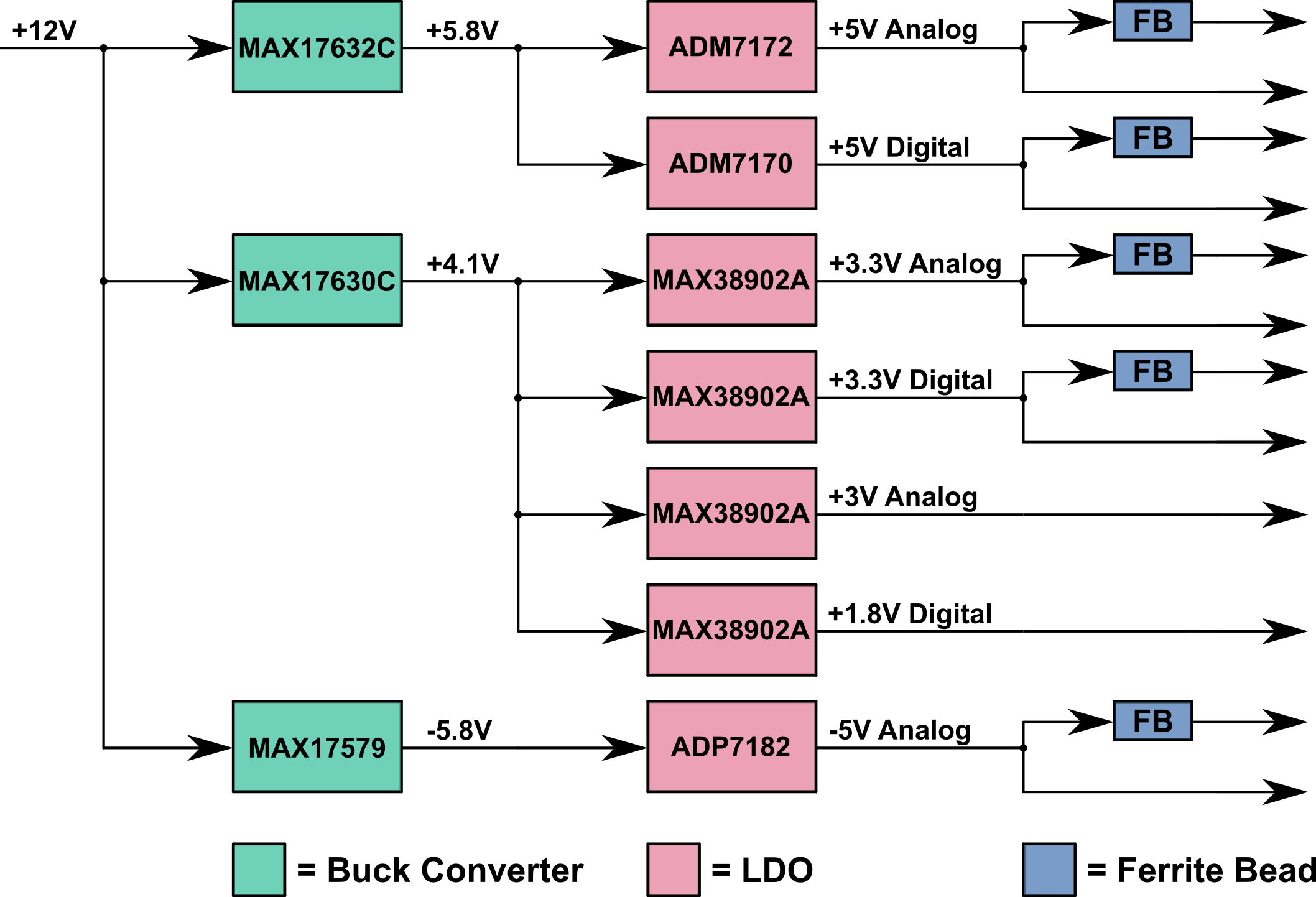
Figure 26 - Power Supply Block Diagram
The first stage are the buck converters that efficiently convert the battery voltage into more manageable voltages. The three buck converters convert the 12V battery output to 5.8V, 4.1V and -5.8V. The voltage outputs were determined by the required headroom from the subsequent low drop-out regulators (LDO) that follow the buck converters. Headroom is the difference in voltage between the input and output voltages of the LDO. For example, the power supply rejection ratio (PSRR) of the 5V LDOs AD ADM717X increase with greater headroom until about 0.65V, so I wanted to aim for a buck converter output of atleast 5.65 V. However, because LDOs are linear regulators, using extremely large headrooms would waste power in the conversion process. But, when the current draw is small, such as for the +1.8V LDO, this wasted power is negligible. To give the input some safety margin, in case of large inrush currents dropping the buck converter output voltages, the target voltages were set slightly higher than necessary.
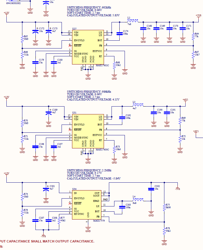
Figure 27 - Buck Converters Schematic
The frequencies for all the buck converters were chosen to be greater than the highest expected beat frequency, 300 kHz, to avoid any switching noise from affecting the measurements. The switching freqeuncies were also spaced by more than 300 kHz so any mixing of the switching noise does not occur at or below 300 kHz. The buck converters are also all operating in constant-frequency PWM which is less efficient to discontinuous-conduction mode (DCM) but operates at a single frequency to avoid any possibility of adding switching noise to the video signal.
Finally, the buck converters were configured to operate for the entire range of expected battery voltages. This is necessary as the battery voltage varies with its charge level. As well, all the component values were calculated from the formulas in their respective datasheets.
Following the buck converters are the LDOs, these provide quieter supply voltages and separation between types of supply voltages. The analog supply voltages are separated from the digital supply lines to prevent switching noise from the digital signals from coupling into sensitive analog components. While the digital supply voltages do not necessarily need to pass through LDOs, to avoid any switching noise from propagating throughout the system, I thought it would be safer to simply regulate all the supply lines near the buck converters. This should prevent any switching noise from coupling onto analog supply lines or from radiating from the digital supply lines.
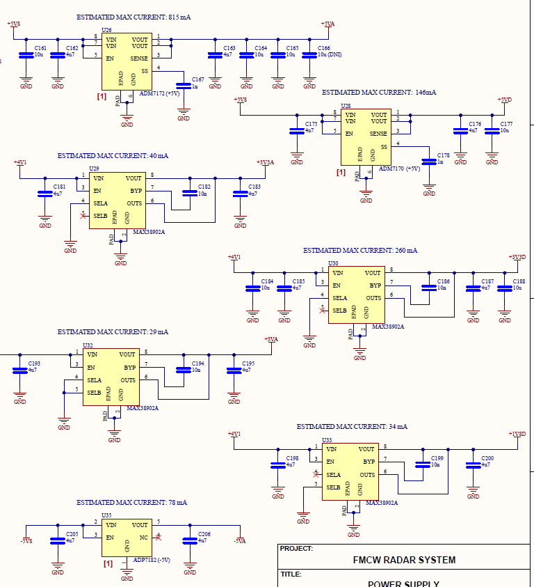
Figure 28 - LDOs Schematic
Finally, the last section of the power supply are the ferrite beads distributed throughout the design preceding noisy and sensitive active components. This also adds another layer of isolation between components, similar to the LDOs, in order to insulate sensitive components from noisy components.
The first consideration to choosing a ferrite beads was to ensure the rated current was well above the current draw being fed through it and to ensure the current draw is within specification after any derating caused by higher ambient temperature. Adding a DC bias to the ferrite will typically move the self resonant frequency (SRF) to higher frequencies. This can cause additional noise to pass through the ferrite at frequencies below the SRF because of its lower impedance.
The next consideration was what frequencies were needing to be attenuated by the ferrite beads. For the RF sections, we'd like attenuation at 5.8 GHz and any switching frequencies. For components with high-speed digital signals, the frequency will depend on the rise/fall times (typically 50 MHz to 200 MHz), while the video/IF sections are mostly concerned with frequencies near the beat frequency. Ideally, the ferrite bead is chosen so the anticipated noise frequency is between the crossover point (where the reactance curve crosses the resistance curve) and the SRF. Furthermore, it should be checked that the ferrite bead does not create any unwanted resonances with decoupling capacitors. In a perfect world, this should be simulated to verify resonances because simple formulas do not account for the parasitics in the system.
One facet I originally ignored about the power supply design was how remarkably the capacitance of Multilayer Ceramic Capacitors (MLCC) change due to its DC bias. If derating from DC bias is not accounted for, your capacitors could perform at half or less of its rated capacitance. This issue was exacerbated because I initially tried to save space by using small packages and tried to keep assembly simple by using non-polarized capacitors such as MLCCs. To resolve this problem, many of the input capacitors with high DC biasing were swapped with polarized tantalum capacitors, whose capacitance is only slightly derated with DC bias. As well, large capacitance MLCCs (1 \(\mu F\) or higher) were replaced with larger package MLCCs whose capacitance does not derate as precipitously with DC bias.
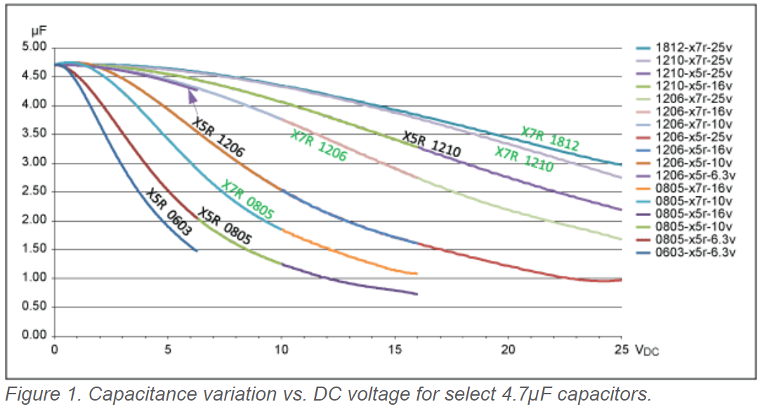
Figure 29 - Capacitance versus DC Bias
Lastly, decoupling capacitors were added to all active component power pins. These capacitors were placed as close to the power pins as possible and each grounded with their own vias.
Antennas
Initially, I was planning on designing my own tapered-slot Vivaldi antennas based on the equations described in Antenna Theory: Analysis and Design [7], however, I was unable to optimize the design to achieve both a good return loss and high gain/directivity. The antenna was simulated in Ansys HFSS and one important note when simulating antennas is to parameterize and link every dimension and geometry of your antenna. This allows the design to be easily adjusted and also it allows your antenna to scale accordingly when a single dimension is adjusted.
Another problem faced when trying to design the antenna was that I was limited in the size of the mesh my computer could simulate. So, I was restricted in the size of the antenna I could simulate or else the design could not be meshed. This severely limited my ability to increase to directivity of the antenna.
Instead of constructing my own antenna, I resorted to purchasing a pair of Vivaldi antennas from Tindie. This antenna has a return loss of less than -18 dB and a gain of 8 dB in the intended operating band which will be sufficient for the project.
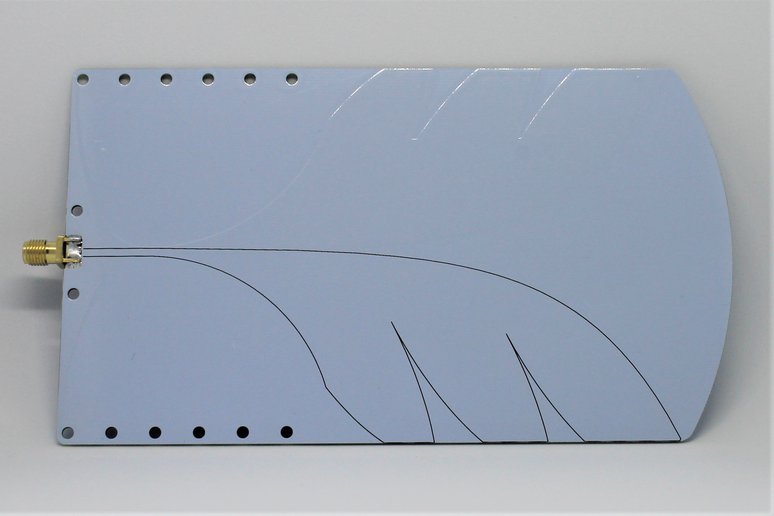
Figure 30 - Wideband Vivaldi Antenna
In the future, I would like to try and design a 3D printed horn antenna with conductive paint.
PCB Design
Layout
With the schematic finished, I could begin on the PCB layout. Before placing the component footprints, I spent time determining the general layout of each functional block, such as the Transmitter, Video/IF Section, Power Supply, etc.
The focus of this process was to separate the noisy blocks from sections that could be susceptible to noise. This meant separating the power supply section that produce low frequency switching noise from the video section as well as separating any high speed digital sections away from the RF receiver or transmitter section. While the design does not include digital signals with rise/fall times that contain significant power around 6 GHz, the precaution was still implemented. The general block placement was determined to be as follows:

Figure 31 - PCB Layout Block Diagram
With the location of each section determined, I began grouping the component footprints into distinct sections. I focused on grouping the main components of each section first with plenty of space between components. With every section grouped together, I began placing each section in their expected location relative to each other.
With a rudimentary placement finished, I iteratively brought the footprints in each section closer together then brought each section closer to its neighbouring sections. With each iteration, the orientation of components were adjusted to line up with the adjacent components. This is simple for intra-section components due to the rats nest indicating the needed traces but for inter-section interconnects, the orientation is more complex and should be given room in case the position needs to be adjusted when the traces are added.
The design also required enough space between each section to allow for interconnects and spacing requirements to ensure acceptable crosstalk between traces. I brought the sections too close to each other initially so during the process of adding interconnects, I had to separate the sections in order to achieve the minimum spacing requirements. Since adjustments will often be required for spacing between sections, it is smart to leave more space than necessary between sections because I found it easier to shrink the design than to expand the design. This stage also feels more like an art because there are several ways to lay out the hundreds of components and tradeoffs for each variation.
Throughout the layout process, I tried to orient the silkscreen designator with the same orientation as the component itself. This helps slightly with the assembly stage to determine which footprint corresponds with which designator.
During the layout process, I noticed the SMA edge mount connector signal pad was much larger than the pads of the preceding component and would be much wider than the projected 50 ohm transmission line width. One method to maintain constant characteristic impedance with a wider transmission line width is to move the ground plane to a lower layer to nullify the increased capacitance from the larger conductor width with greater conductor spacing. However, to forgo this additional work needed to simulate a modified footprint in an EM simulator, I switched to a connector with a narrower center signal pad.
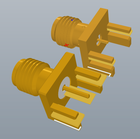
Figure 32 - Edge-Mount SMA Connectors
The new connector pad will not be matched perfectly to 50 ohms, so I still tried to minimize the microstrip transmission line length before this impedance discontinuity so reflections would not significantly degrade the signal integrity. In designs where the connector pad or the connecting transmission lines are a significant portion of the signal wavelength, it would be important to simulate and optimize the footprint or find a better connector that improves the matching to minimize reflections.
PCB Manufacturer
Before beginning the routing of interconnects between components, I needed to establish the PCB stackup in order to calculate the trace width for a 50 ohm transmission lines.
The two main PCB manufacturers I looked at for this project was JLCPCB and OSH Park. I investigate these two manufacturers because I've used them previously but there are many others companies that would be worth investigating as well.
JLCPCB provides extremely affordable PCBs and works with component sourcing distribution company LCSC so both PCB and components can be purchased at the same time. LCSC is often cheaper than other component distributors such as Mouser and Digikey for generic components but can sometime be more expensive for more unique components. A very useful feature of LCSC is that the components can be installed by JLCPCB, so you don't have to assemble the board yourself.
OSH Park is a US PCB manufacturer that provides quick prototyping to customers in North America. The base capabilities are superior to JLCPCB but JLCPCB can be configured to have equal or even better manufacturing capabilities compared to OSH Park for an increased cost. OSH Park is more expensive per PCB compared to JLCPCB.
Since OSH Park had more information about their stackup material and provided the dielectric constant for both their substrate and soldermask, it was chosen as the PCB manufacturer. These values are needed to determine the line width of transmission lines. OSH Park also allows for a wider 50 Ohm transmission line which reduces impedance discontinuities with component pads that are often wider than the transmission line.
OSH Park also provides an easy Altium Design Rule file that you can be added to the project so all design rule checks are in line with OSH Park's manufacturing capabilities. OSH Park also uses slightly lower loss (lower dissipation factor) prepreg in their PCB stackup than JLCPCB. JLCPCB has started providing Rogers and PTFE substrates for ultra low loss PCBs which would be appealing to use but at the time of the design, they only provided these substrates in 2-layer designs.
Routing
Analog Interconnects
The first task to routing the analog sections was to determine the required line width to achieve a matched characteristic impedance for the PCB transmission line. With the board stackup defined, I used the Altium 2-D solver to determine the microstrip trace width for a characteristic impedance of 50 ohms, which is the input/output impedance of most RF components.
For the design, I used microstrip transmission lines for the RF sections of the PCB because it facilitates simpler routing. With microstrip transmission lines, I don't need to worry about adjusting adjacent grounds around component pads that would be required for coplanar waveguides transmission lines and I would not need to simulate impedance discontinuities resulting from vias required for stripline transmission lines. While microstrip transmission lines may not contain the EM fields as well as the other types of transmissions lines, the thin separation distance between the signal conductor and return plane, employing via fencing and using an EMI can should sufficiently contain fields to avoid performance degradation.
Operating at 6 GHz, via stubs from stripline transmission lines are not too impactful but if operating at much higher frequencies where via stubs are an appreciable portion of the signal wavelength, they must be considered.
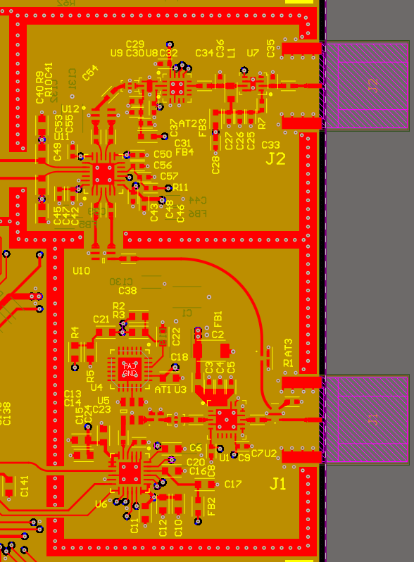
Figure 33 - Transmitter and Receiver Top Copper
Another aspect I investigated was whether the solder mask should be removed above the microstrip transmission line. Removing the solder mask in theory would reduce the dielectric loss, therefore lower the signal attenuation loss per inch however, if the solder mask is removed, the copper trace will instead be plated to avoid oxidation and improve solderability which can also effect the signal. OSH Park uses Electroless Nickel Immersion Gold (ENIG) plating but this plating layer adds additional losses due to its ferromagnetic properties of nickel and often rougher surface than the laminated copper. So which method provides less loss? This question was investigated by Hao He and Rongyao Tang [8].
In the paper, they investigate magnitude and phase of insertion loss (S21) associated with different PCB surface finishes. While they use coplanar waveguide transmission lines for their testing, I expect the attenuation versus frequency characteristics to behave similarly for microstrip transmission lines. In Figure 6 of the paper, they show that the ENIG finish experienced more loss than the same coplanar waveguide with a solder mask above ~1 GHz.
Since the solder mask will not greatly affect signal attenuation compared to ENIG plating and the solder mask helps keep the solder paste from spreading away from the component pad, I decided not to remove the solder mask over any microstrip transmission lines.
For all the RF traces, I conformed to the following:
- Keep traces as short as possible to minimize effects from impedance discontinuities and minimize insertion loss.
- Maximize the bend radius to keep a constant characteristic impedance.
- Maintain uninterrupted ground plane under the microstrip signal trace.
- Use tapered transitions (teardrops) between the transmission line and component pad as required.
- Route away from any components or traces that could disrupt EM fields or are noisy.
The same principles were used for the routing the video/IF section, however the rules above are not as crucial because the signal's wavelength is so large compared to the trace lengths.
One unanswered question I had about the tapered transitions between the transmission line and component pads is whether it is actually worthwhile for the short traces in the RF sections. If instead, I used microstrip lines that had the same width as the pad (thus having a much lower or higher characteristic impedance) would it be as effective? Or, because the traces are electrically short, the tapered transitions provide no benefit at all. This is something I hope to investigate further in the future. In the ideal scenario, all component pads would have the same widths as the 50 ohm microstrip transmission line width so there are no impedance discontinuities. This could be done by tailoring pad sizes to match a 50 ohm trace or adjusting the stackup characteristics such as the thickness of the substrate or dielectric constant of the substrate in order to adjust the transmission line width.
There are also cases where the component pads were smaller than the 50 ohm microstrip trace width so I was unsure if teardrop transitions are required to decrease the trace width or if the trace could just be started directly at the pad. I'd speculate that starting the transmission line directly at the smaller width pad would create a resonant structure similar to via stubs. Since the excess copper is so electrical small, they would resonate at frequencies much higher than the operating frequency range.
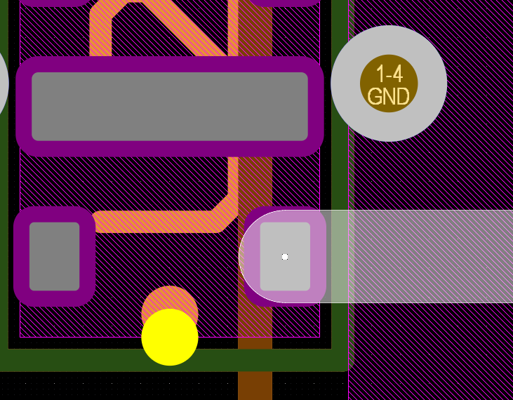
Figure 34 - Transmission Line Width Larger than Component Pad
For differential signals, I length matched the differential pair to minimize any phase differences between the two conductors. While, this is particularly important for the RF signals, I'm not certain how important this was for the video/IF signals.
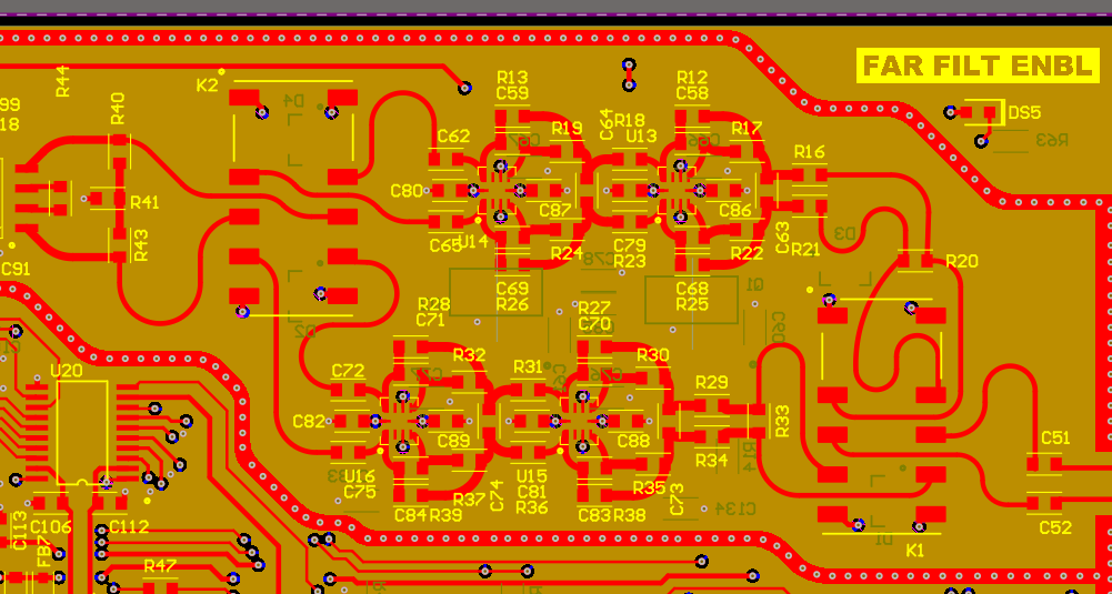
Figure 35 - Video/IF Differential Length Matching
Since, the video/IF signal phase would change relatively little for the lengths used in the design, the traces could have been routed directly to the components but this will need to be further investigated.
Power Supplies
The traces between the power supply components are relatively straight forward since they only contain DC voltages. When possible, copper polygons were used to connect pads to lower resistance and inductance.
In order to minimize breaks in the ground planes on layers 2 and 3, power planes were not used. Instead, power rails consisting of wide traces were used to deliver power to all components in the design. The minimum trace width for the required power consumption of the voltage rail were found from Saturn PCB Toolkit.
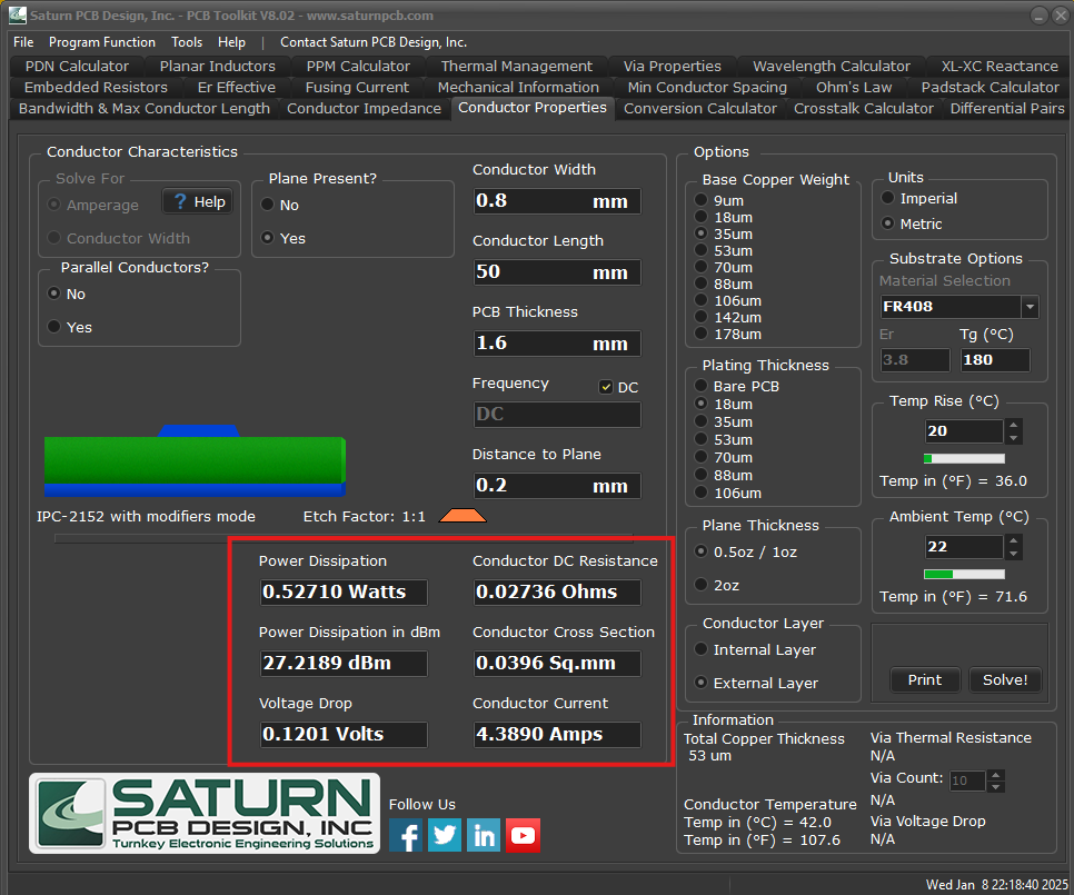
Figure 36 - Saturn PCB Toolkit
Using traces rather than power planes will increase the power supply inductances significantly, but the high frequency components that are most affected by the elevated inductances should be eased by the decoupling capacitors near the component power pins. Additional decoupling capacitors were used at all high-speed and RF components and unpopulated capacitor footprints were employed in case additional decoupling capacitors are necessary. After completing all the routing, the power traces were also increased as wide as possible to try to diminish the PDN resistance and inductance.
Test points were added throughout the design in order to verify the power supply voltages during power up. Since the conductors only contain DC voltages, I did not need to worry about changes to impedances resulting from these test points however for high-speed digital or RF signals, the designer must be cautious to not degrade signal integrity by including test points.
The power delivery network (PDN) was one of the features of the design that was lacking proper analysis. Ideally, the PDN could be simulated to ensure it behaves without any reduction in performance so this will be a topic for future investigation.
Digital Interconnects
Most of the digital interconnects in this design are low speed control signals which can be routed without much consideration about signal integrity. However, there were two interfaces that required careful consideration, the ADC DCMI interface and the USB HS ULPI interface.
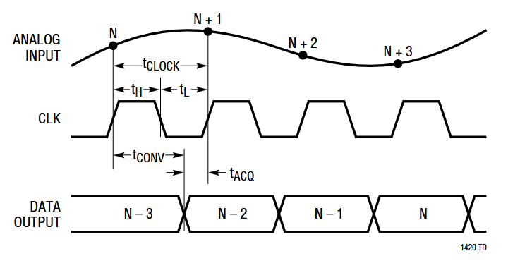
Figure 37 - ADC Timing Diagram
The ADC parallel outputs are updated after two clock cycles followed by a conversion cycle of 70 ns typical (90 ns maximum). If we assume a 50% duty cycle clock signal and 4 ns rise and fall times, the output data will be valid for 28 ns prior to the third clock cycle and 68 ns after the third clock cycle. However, with a worse case conversion time of 90 ns, these times changes to 8 ns prior to the third clock cycle and 88 ns after the third clock cycle. So it was imperative to verify that with the additional trace delay and component propagation delays, the ADC data can be sampled by the MCU in typical and worse case scenarios.
The trace delay from clock buffer, TI LMK1C1102, to the ADC clock input is 253 ps and trace delay from clock buffer to the MCU DCMI clock input is 136 ps. With a maximum voltage-level translator propagation delay of 4 ns, the total delay from clock buffer to ADC clock input is 4253 ps. So the MCU would read the DCMI inputs 4117 ps before the clock signal arrives at the ADC. Note that all these rough calculations disregard the delay through vias and the output to output skew of the clock buffer and voltage-level translators but with higher speed signals where several picoseconds are significant, these times should be considered.
The longest ADC output trace is D7 and will have a worst case propagation delay of 4419 ps from the ADC to MCU DCMI input. Therefore, with a 90 ns ADC convertion time, a 4.1 ns skew from the ADC clock to MCU DCMI clock and a 4.4 ns propagation delay on trace D7, the required 2 ns setup time for the MCU DCMI timing specification would not be met.
Instead of length tuning the traces to meet the timing requirements for worst case delays, the MCU DCMI interface can be configured to sample at the falling edge of the clock signal. Avoiding length tuning also helps to minimize board space because tuning patterns occupy a relatively large space. With an ADC conversion time of 70 ns there is around 18 ns of acquisition time using the falling edge but with this method, the skew between the ADC clock and DCMI clock adds to the available acquisition time because it shifts the sampling point ahead by 4.1 ns. This will essentially cancel out the propagation delay of the ADC outputs. For longer ADC convertion times, the acquisition time would simply increase. Therefore, sampling with the falling edge should ensure sufficient setup and hold times for DCMI sampling.
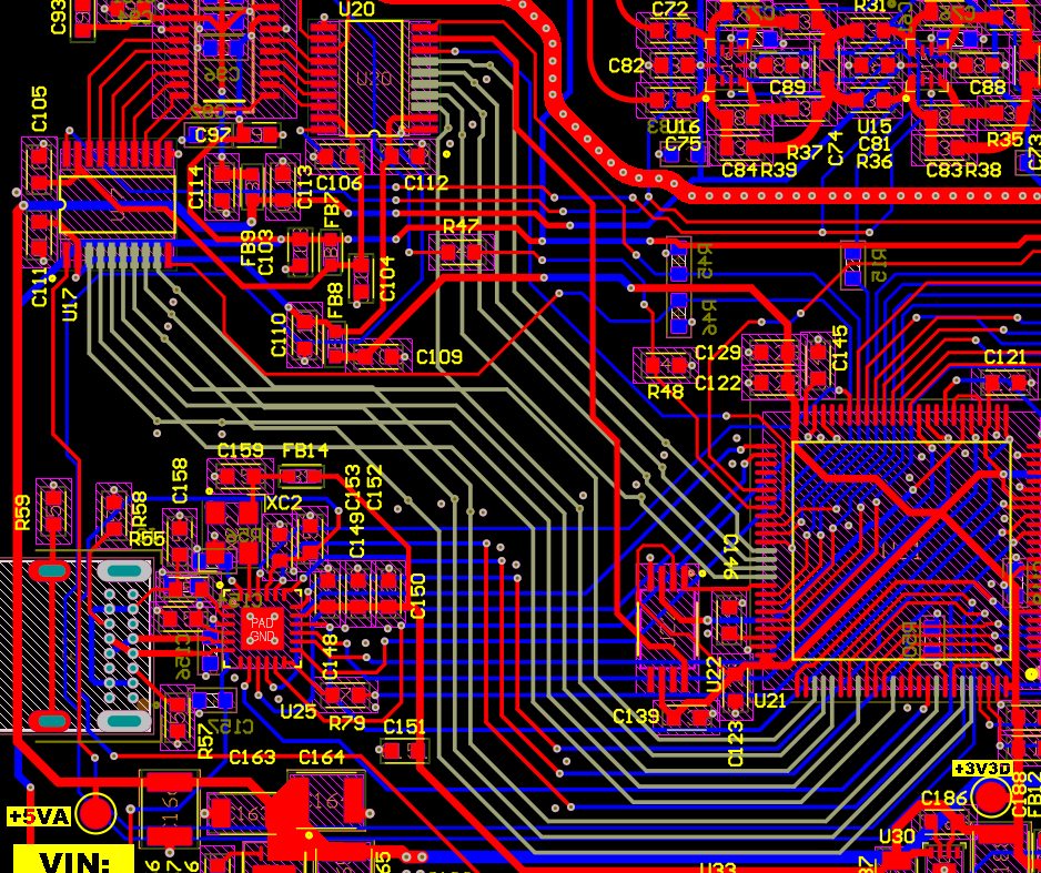
Figure 38 - DCMI Interconnects (highlighted in grey)
The other interface that required special care was the ULPI interface between the MCU and the USB HS transceiver. Typically, the MCU or SoC OEM will provide a maximum trace length and maximum trace-to-trace skew for routing ULPI interconnects but STM did not provide one. Rather, they provided a minimum setup and hold time in their clock timing specification. Microchip does state that ULPI trace lengths should be limited to 3 inches maximum, so I abided with this requirement instead. For the trace-to-trace skew requirement, some OEMs recommend 100 ps but the maximum skew from this design is around 170 ps which should be acceptable as the setup and hold time requirements will still be met.
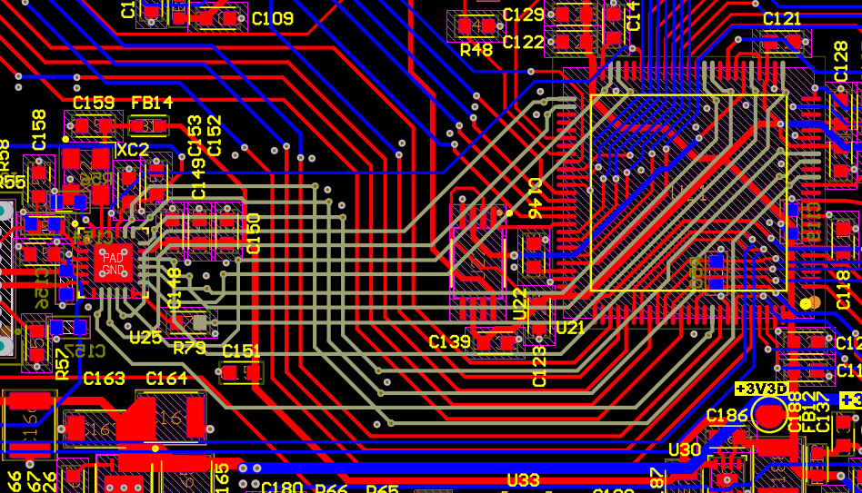
Figure 39 - ULPI Interconnects (highlighted in grey)
Some documentation recommend adding series termination resistors on the DATA, STP and CLK lines to improve signal integrity. Since the DATA and STP lines will be driven inclusively by the MCU, which has a minimum rise time around 4 ns, the impedance mistmatch should not cause any signal integrity problems.
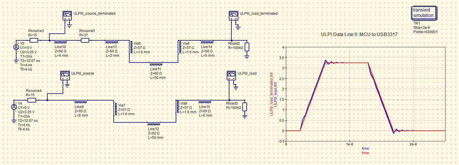
Figure 40 - QucsStudio, ULPI Data Line With and Without Series Termination
However, the clock will be driven by the USB transceiver which could have a much lower rise/fall time so after simulating with its expected rise/fall time, it was decided a 37 Ohm series termination would improve its signal integrity.
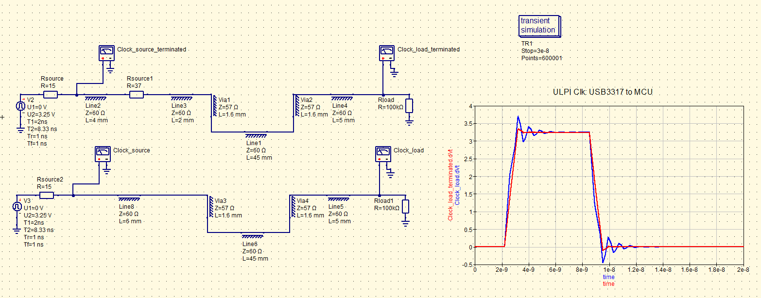
Figure 41 - QucsStudio, ULPI Clock Line With and Without Series Termination
The trace width for the high-speed digital signals is 0.3 mm which has a characteristic impedance of around 60 ohms. Since the input and output ports of the digital components are not 50 ohms, the traces do not necessarily need to be 50 ohms. As well, if 50 ohm traces were used, I would require much more area to maintain the same coupling factor between traces because the traces would be wider and thus separation distance would be wider. For high-speed digital signals, I tried to maintain a separation distance of 2 track width between traces (0.6 mm). Per Eric Bogatin's testing with 50 ohm tracks, a separation of 2 track widths resulted in a 2.5% coupling factor which is acceptable for this design. In order to achieve this separation distance, I had to increase the distance between sections which requires a surprising large amount of time compared to shrinking the section-to-section distance. This coupling factor was also simulated in QucStudio which was found to be slightly larger than 2.5%.
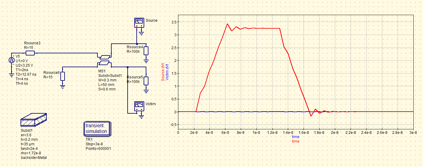
Figure 42 - QucsStudio, Trace Coupling
Return current vias from ground layer 2 and 3 were added near high-speed digital signal vias to add a means for return currents to transition between layers. I tried to add a return current via for each high-speed digital signal in order to reduce common impedance coupling but where there was a lack of space, a single return current via was used for multiple signal traces. I never simulated at exactly what rise/fall time a return via is needed and when return current can pass through the capacitance of the adjacent ground planes but this should be investigated further.
While routing the interconnects, I started with the most crucial and high-speed interconnects first so that they could be routed directly without any obstructions. The low speed control signals were then routed around these high-speed signals. At this point, I also had to re-assign some control signal pins on the MCU to avoid unnecessary vias and to use pin locations that could provide as direct of an interconnect as possible to its destination. In the future, I'd like to try the auto routing feature to speed up routing low frequency digital signals where signal integrity is of minor importance
Additional PCB Structures
After completing all the routing, via fencing was added around the RF transmitter front-end and receiver front-end sections
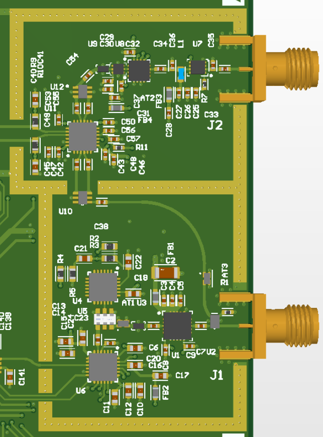
Figure 43 - RF Section Via Fence
The via fence separation was set to be less than 1/20 the highest wavelength. Using a maximum frequency of 6 GHz, and an effective dielectric constant, (\(\epsilon_{eff}\)), of 3.2, the vias should thus be spaced a maximum of 1.4 mm. Most vias were separated by 1 mm but many vary in separation distance to let traces pass between the ground vias.
The solder mask was also removed above the via fence so EMI shielding cans can be soldered onto the PCB. Technically, you only need the EMI shield on the receiver section, but it was added to the transmitter section just to investigate if it improved performance. To reduce space, I did not use the shielding clips but this would be helpful so the EMI can can be removed easily. However, when using EMI cans, you'll need to find a EMI can that has similar dimensions to your design. By contrast, I will most likely construct my own EMI can using non-adhesive copper tape, so I can shrink the design as much as possible without any constraints on the pads for the EMI can.
A via fence was placed around the IF/video section as well to minimize noise from other sections of the board, specifically the low frequency switching noise from the buck converters. However, I believe the 1/f noise and thermal noise will probably dominate at the ADC input, but it would be interesting to determine the actual noise reduction of implementing the via fence. The solder mask was not removed for this via fence because I'm not planning on using EMI cans for this section since the trace lengths used should not be able to pick up significant noise in the video/IF operating frequencies.
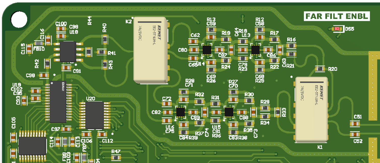
Figure 44 - IF/Video Section Via Fence
Another feature added was a large exposed ground pad under the PA in case a heat sink is needed for heat dissipation. The copper was exposed not for grounding purposes but I believe a conductive surface would presumably conduct more heat to the heat sink.
Finally, I added some mounting holes at the four corners and silkscreen comments about the input voltage, LED descriptions and TX and RX indication arrows.
Future Work
The PCB and components have been ordered and will be assembled and tested soon. I always order the parts before ordering the PCB to ensure the components can be obtained and footprints don't need to be changed due to part unavailability or obsolescence.
In the future, I hope to swap the MCU with an FPGA that could process the data directly on the PCB. This would avoid any throughput restrictions causing limitations in the sampling rate of the ADC and would also avoid the need to store large amounts of data on the PC before processing it.
Additionally, I would like to expand on the simulations and computer aided analysis such as for the PDN to verify parasitics do not impede performance and sufficient decoupling capacitors are used. Furthermore, proper noise analysis on the IF section would be useful so the noise figure of the entire receiver section can be determined. As well as further analysis on the ADC performance and the effects of the IF length matching.
One question that came up while routing some QFN packages was whether it is better to connect all the ground pins to the center pad or give each ground pin its own via to the ground plane (or a combination of both methods). In my opinion, having every QFN ground pin connected to the ground plane through their own via could cause ground noise due to potential differences on the ground plane. Yet, if all ground pins are connected to the center ground pad, there would be an increase in inductance because all the return currents will be going through the same ground vias. I hope to investigate this further to understand the optimal grounding method for these QFN packages.
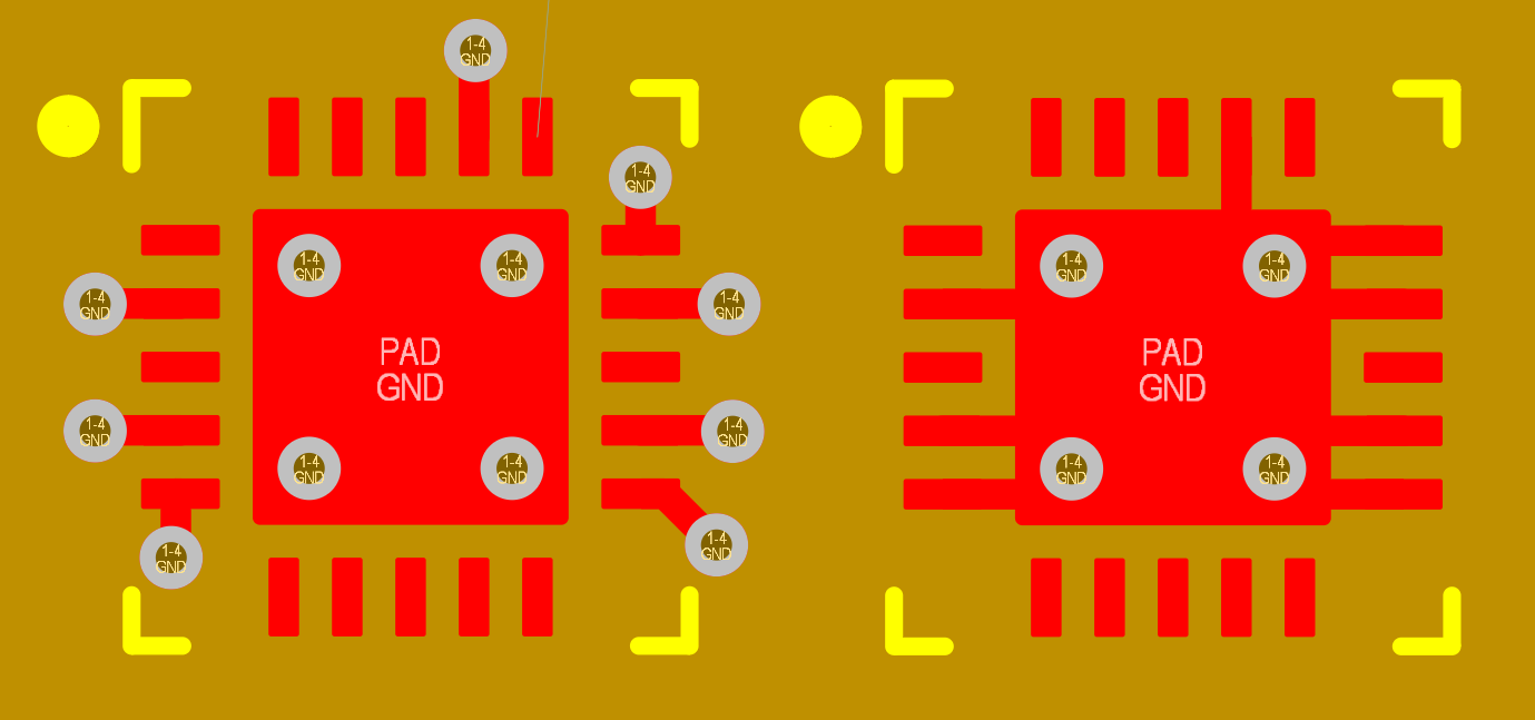
Figure 45 - QFN Grouding Methods
Lastly I would like to work on my own directional antenna to be used for this project, but this might have to wait until I get an upgraded computer that can support larger simulation meshes.
Mistakes and Lessons Learned
One noticeable mistake I identified after sending the fabrication files to OSH Park to manufacture the PCB was that some clusters of vias created large breaks in the ground plane.
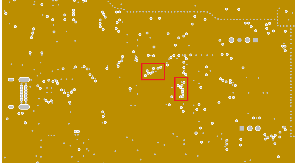
Figure 46 - Ground Breaks from Vias
This was mostly spotted around the MCU as a result of fanning out the high density of pins. This will cause the return currents to take longer paths and add parasitic inductance and could degrade signal integrity. Luckily, most of the breaks in the ground planes are near slower rise/fall time digital signals that should not be greatly affected by these breaks in the ground plane. For following projects, this will be considered.
Another mistake was treating the first page of the schematic as a hierarchical diagram when it was set up as a flat design. The hierarchical structure was chosen to show interconnects between different sheets, but I believe I incorrectly configured it as flat multi-sheet design. This led to several warning messages in Altium, but they were suppressed by changing the project options or disabling the messages.
An important lesson learned throughout this project was accepting some uncertainty in the design as a way to move onto the next step in the process. It can be hard to progress when you know that a design is not as optimal as imaged so it can cause you to get stuck but sometimes you need to take the risk of lowered performance and uncertainty so the project can be completed in a timely manner.
Conclusion
The entire schematic, 3D PCB and PCB copper layers are embedded below.
References
[1] Henrik's Blog, https://hforsten.com/
[2] Minimal Measuring Range, https://www.radartutorial.eu/01.basics/Minimal%20Measuring%20Range.en.html
[3] George W. Stimson, Introduction to Airborne Radar, 3rd Edition, 2014
[4] Gregory L. Charvat, Small and Short-Range Radar Systems, 2014
[5] Warren L. Stutzman & Gary A. Thiele, Antenna Theory and Design, 3rd Edition, 2012
[6] Arthur B. Williams, Analog Filter and Circuit Design Handbook, 2014
[7] Constantine A. Balanis, Antenna Theory: Analysis and Design, 4th Edition, 2016
[8] Hao He & Rongyao Tang, Effect of Permittivity and Dissipation Factor of Solder Mask upon Measured Loss, https://www.ipc.org/system/files/technical_resource/E39%26Rongyao%20Tang.pdf