Overview:
- Assemble DDS based Signal Generator PCB using a reflow oven.
- Write an AD9834 driver to interface with a STM32 microcontroller.
- Verify operation and output of the Signal Generator PCB.
Table of Contents
Introduction
With the DDS PCB Design completed, it was now time to manufacture the board, assemble and test the design. In order to test the design a driver library was required for the AD9834 so instructions can be sent to the IC from my STM32 microcontroller.
Manufacturing
The PCB was manufactured by JLCPCB using the JLCPCB Stackup JLC04161H-3313. JLCPCB was the most affordable manufacturer available at the time. I followed Phil's Lab KiCad tutorial to generate the proper files and then uploaded them to JLCPCB. The following manufacturing settings were chosen.
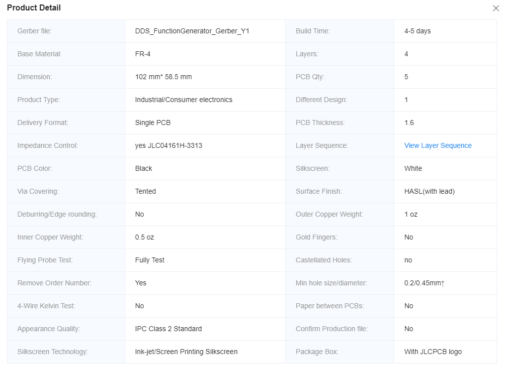
Figure 1 - JLCPCB Settings
The minimum order quantity was 5 and they arrived 19 days after the order was submitted.
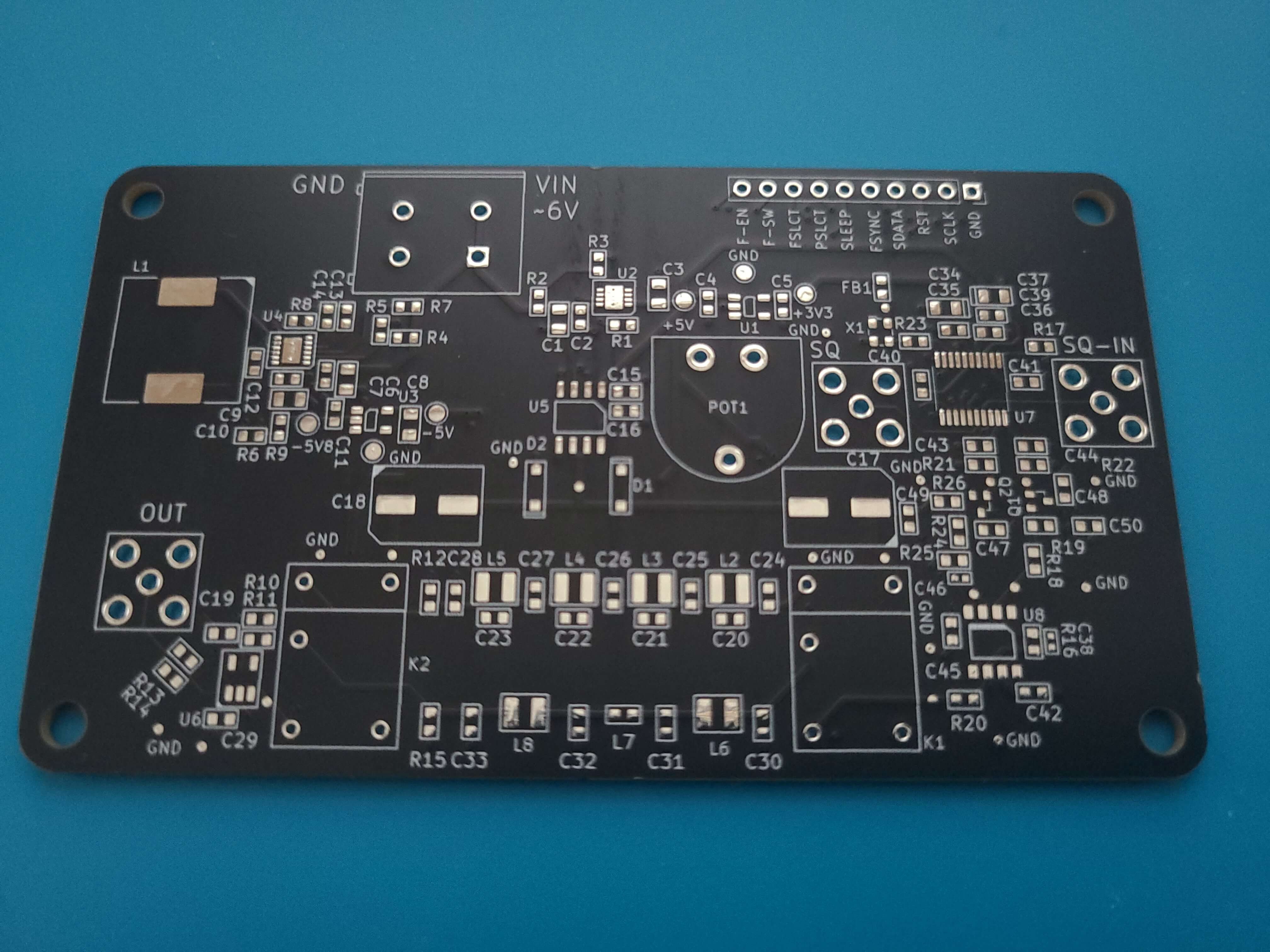
Figure 2 - Bare PCB
A solder stencil was ordered along with the PCB so solder paste and a reflow oven can be used for assembly.
Assembly
Components for the PCB were purchased from Mouser. A Bill of Material (BOM) was created in KiCad and uploaded to Mouser's BOM tool. This method allows us to upload an Excel file to Mouser and add all components to the cart without needing to search for each individual component. A few components were out of stock and acceptable alternates were chosen as replacements.
The Surface Mount Technology (SMT) components were soldered onto the PCB using solder paste and a reflow oven. The reflow oven was built from a free Facebook Marketplace toaster oven and an Arduino Nano. The design was based off the Whizoo Reflow Oven.
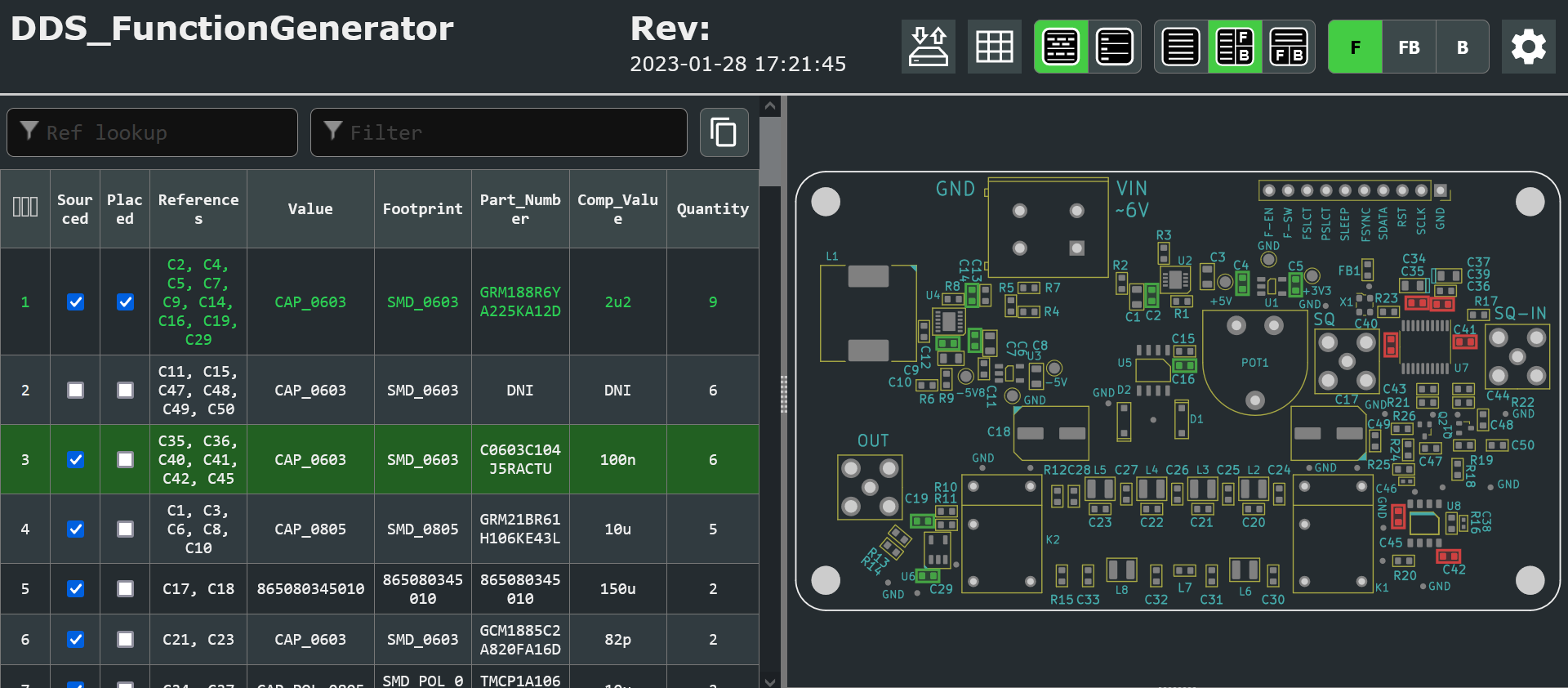
After applying solder paste to the PCB the components were added starting from the smallest components first, 0603 components, and finished with the largest components. The KiCad Interactive HTML BOM tool was used to mark components complete when added and determine component item number and part number.
Figure 3 - Interactive HTML BOM
Before starting assembly, I sorted the components by item number which allowed me to easily find each component when placing them on the PCB.
Unused PCBs were placed around the main PCB and the solder stencil was taped down in place. Solder paste was applied to the stencil then squeegeed using an old laundry card. The first attempt to solder the components onto the PCB turned out awful because I applied too much solder paste. This caused many of the QFN package leads and SOIC package leads to short together. I also forgot to place the large capacitors for the filter switch mechanism. A hot air gun will be used to rework the improperly soldered components and add the large capacitor.
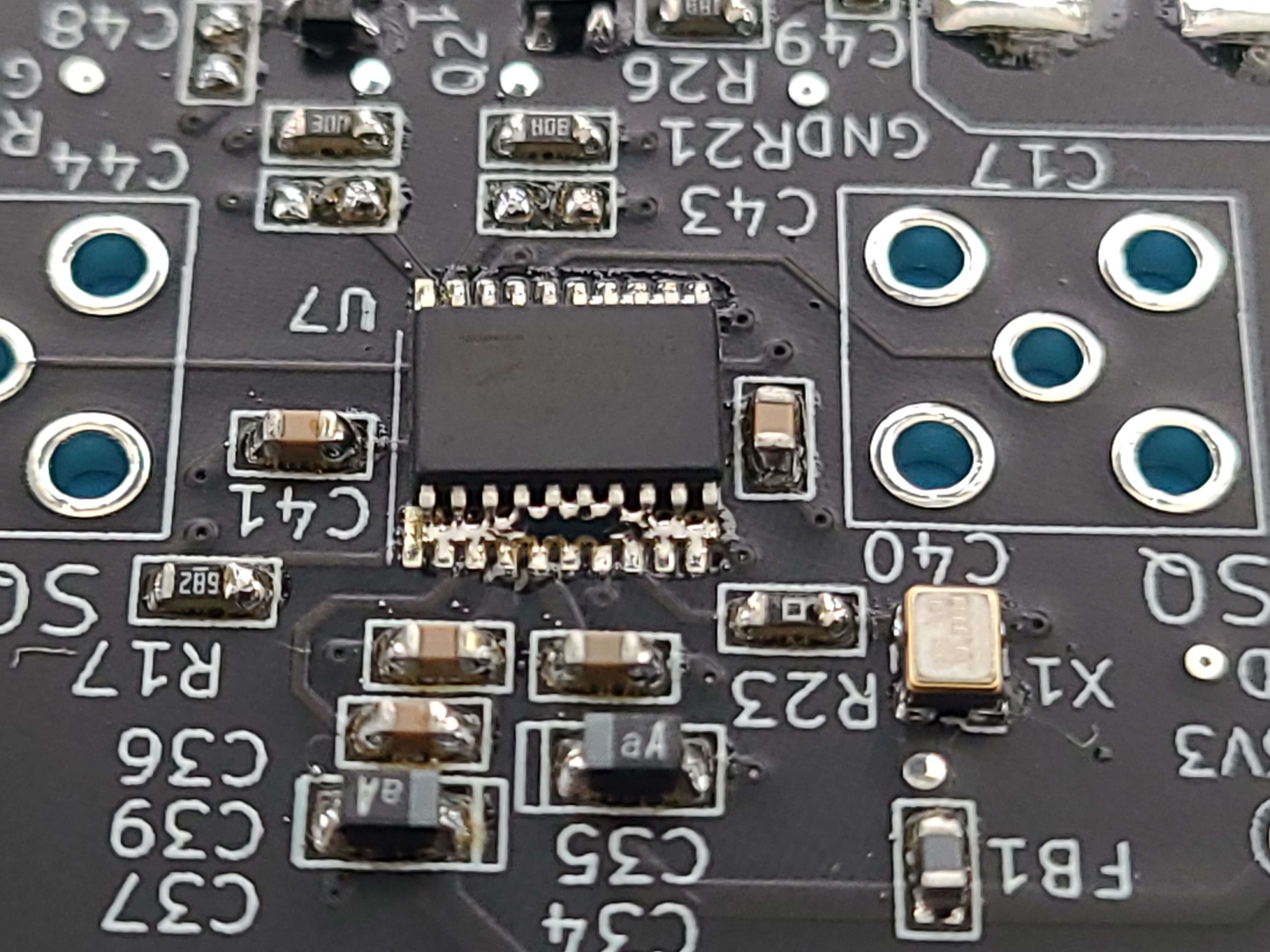
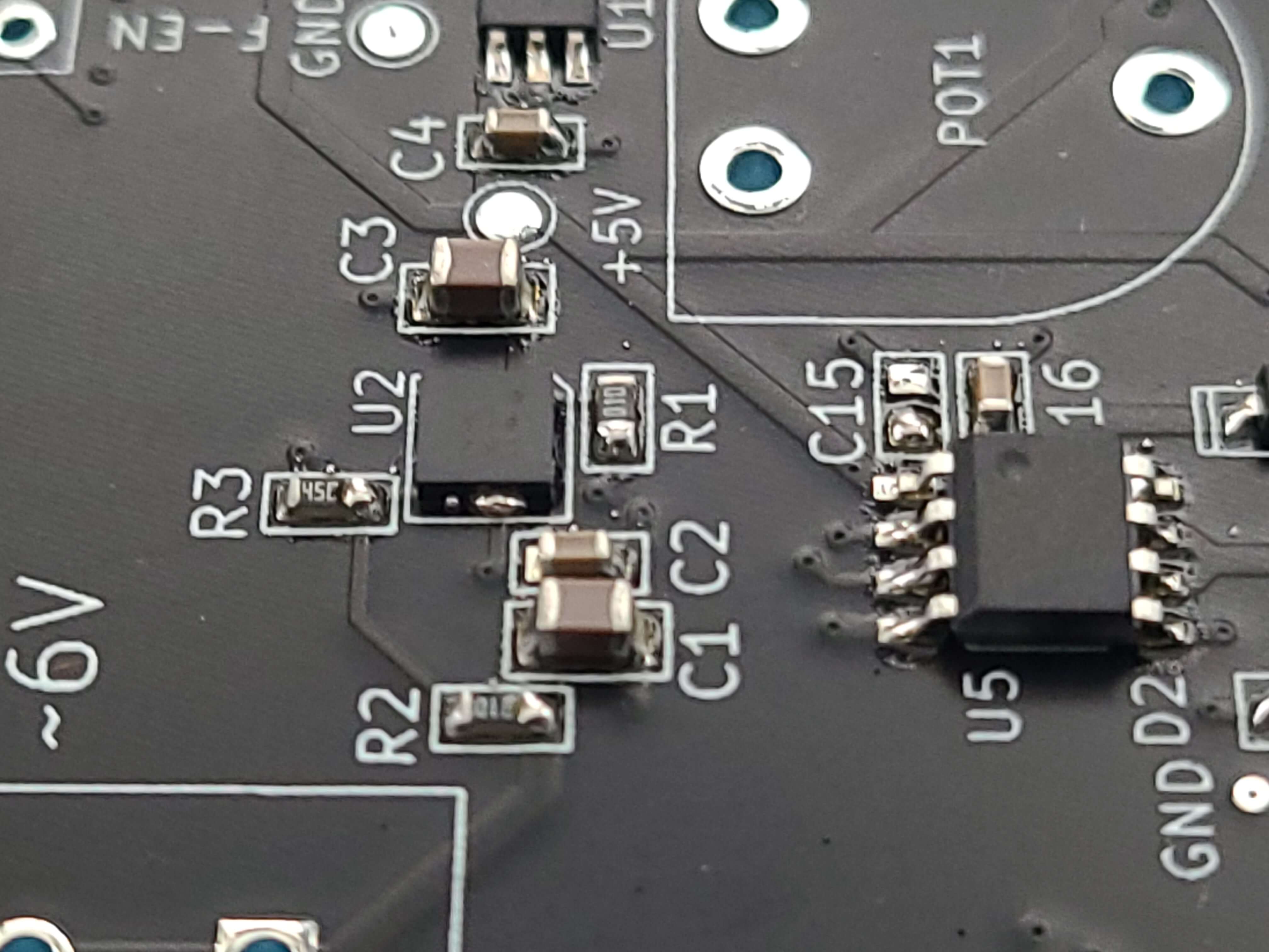
Figure 4 - Reflow Soldering 1st Attempt
On the second attempt, after applying the solder paste, I passed over the stencil again with the card with a steep angle and lots of pressure to remove any excess solder paste. After placing the components on and using the reflow oven, the solder joints turned out great.
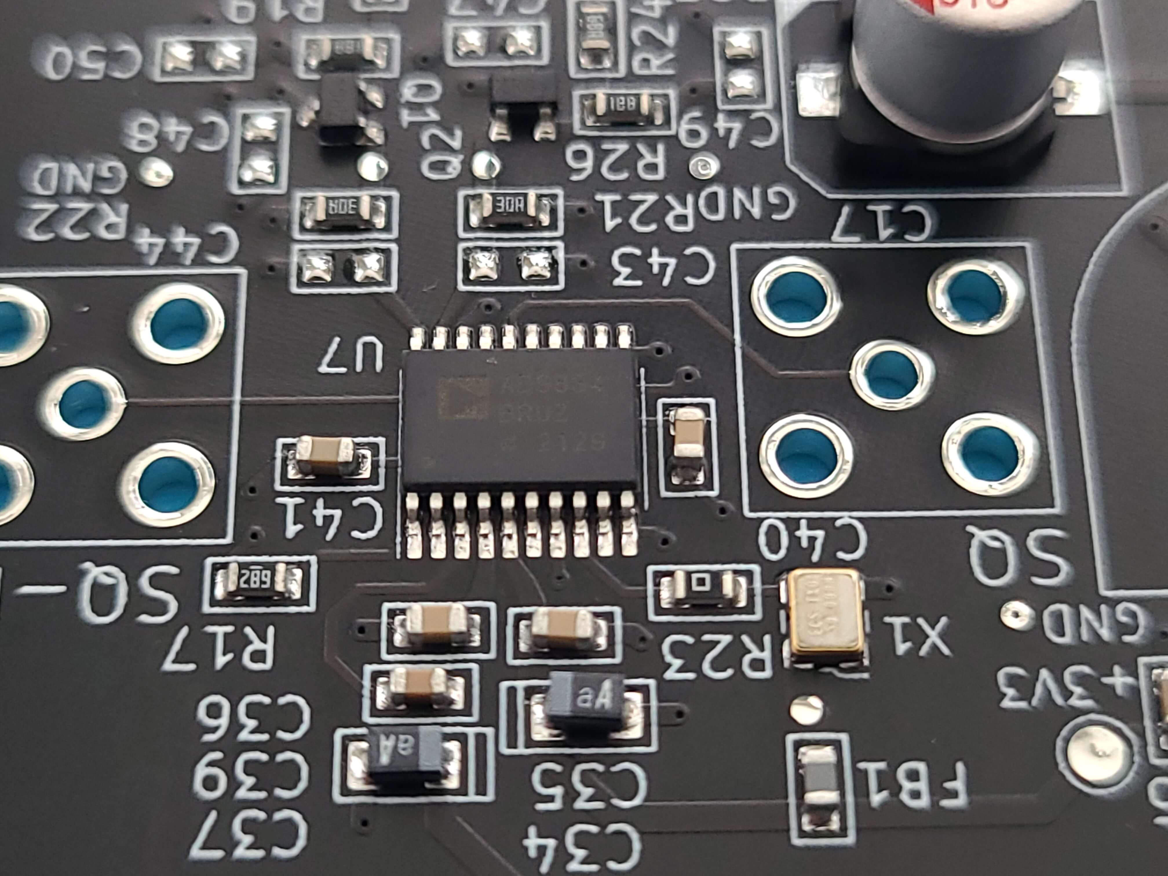
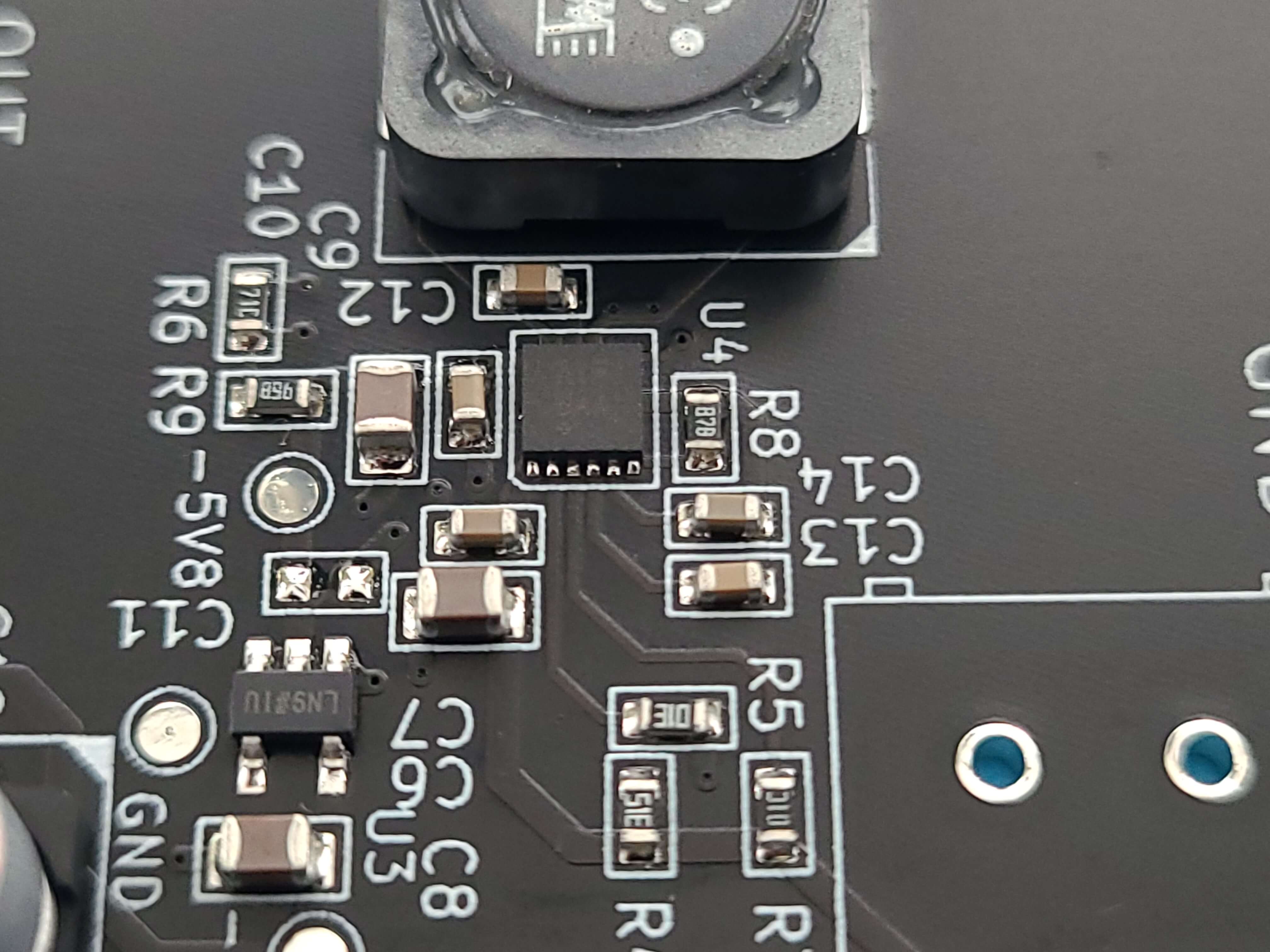
Figure 5 - Reflow Soldering 2nd Attempt
After hand soldering the through hole components and adding the standoffs the final PCB was fully assembled.
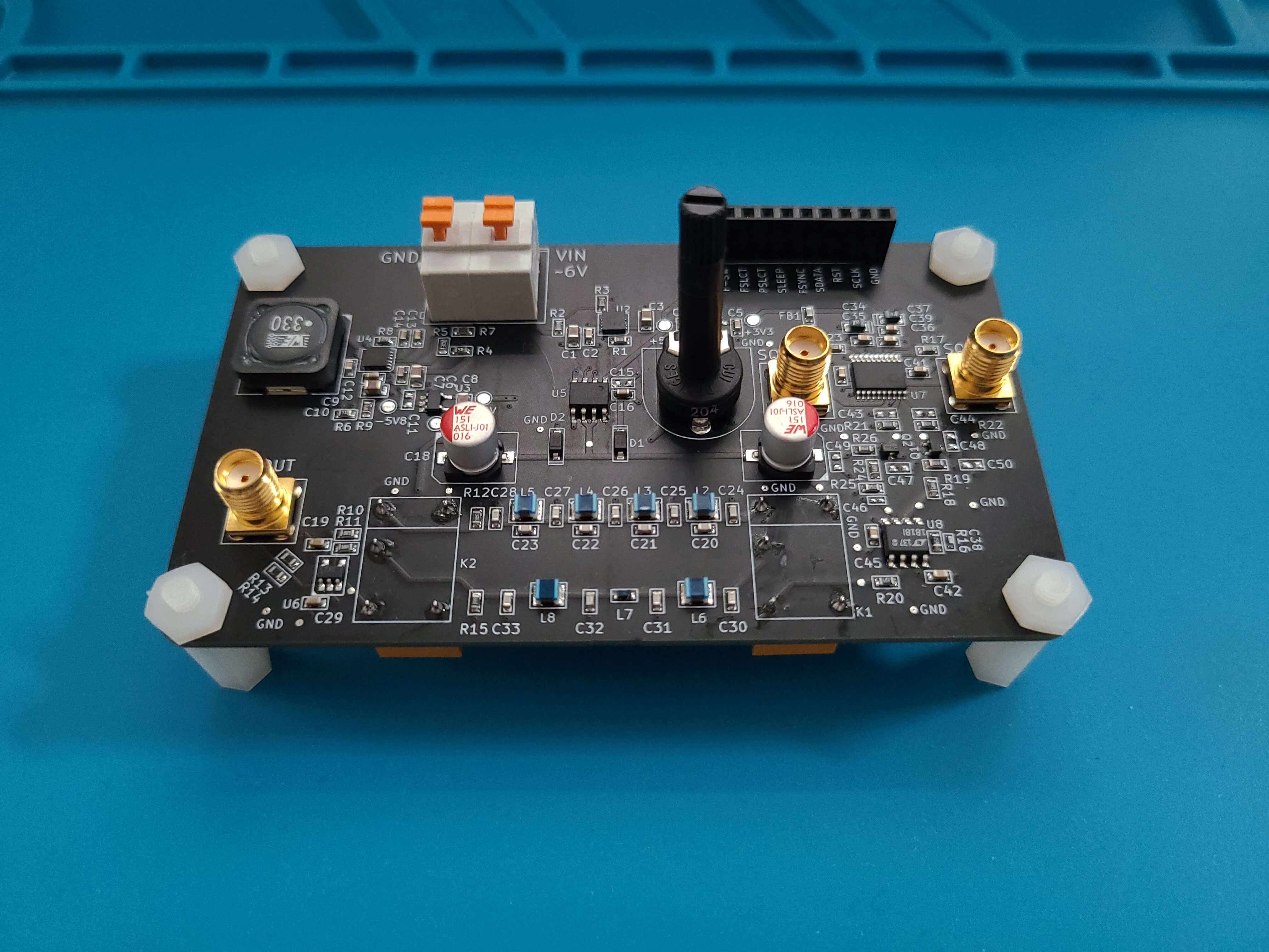
Figure 6 - Fully Assembled PCB
Now you may notice that the relays are upside down and wonder why I would design it that way, and the answer is that they are supposed to be on top. PCB footprints for SMT components are always from the top view however for some through hole components, such as the relay DS1E-SL-DC5V, the datasheet specified the footprint from the bottom view. Luckily the standoffs were long enough to allow the bottom placement of the relay without affecting the usability of the design. This issue could have been avoided if 3D models were added to the PCB footprints.
AD9834 STM32 Driver
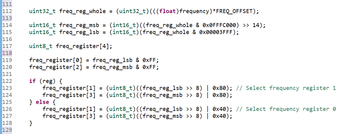
In order to communicate with the AD9834, a driver library was created for the STM32L4 microcontroller. The driver was created in STM32CubeIDE and uses functions from the STM32 Hardware Abstraction Layer (HAL) drivers. The driver includes functions to switch output waveforms, set frequency and phase and switch between frequency and phase registers. The driver was designed so a connection struct could be passed to each function and the struct contained all the required connection and control signal information needed.
While setting up the SPI communication parameters in STM32MXCube I learned that when using the STM32MXCube configuration Clock Polarity (CPOL) High and Clock Phase (CPHA) 1 EDGE, the clock line does not get set high until after you've sent an SPI command. If a pull-up resistor isn't placed on the clock line, the line will stay low until after your first command. This caused some confusion because the AD9834 requires the clock line to be high when the FSYNC (equivalent to SPI NSS line) line goes low or else the AD9834 won't read the incoming data correctly.
Figure 7 - AD9834 SPI Timing Diagram
To fix this I just send the first command twice. Once the first command is sent, the FSYNC line is held high when idle.
Another part I had difficulty with was the proper placements of bytes in the data buffer for multi-word SPI transmission. For example, the microcontroller can update the full 28 bits in the frequency register to set the output frequency of the AD9834. However, the AD9834 uses 16 bit words so 2 consecutive words must be sent to set all 28 bits in the register. The AD9834 requires the Most Significant Bit (MSB) to be sent first and uses 16 bit words so the following SPI configuration was used in STM32MXCube.
Figure 8 - SPI Configuration
Per AD9834's datasheet, to set the full 28 bits of the frequency register the control register bits must be configured first then the 14 LSBs can be sent followed by the 14 MSBs of the desired frequency. The HAL function HAL_SPI_Transmit(...) used to transmit data using SPI requires the data to be passed as an array of bytes. So, with the microcontroller setup with MSB first, should the first 16 bit word (the frequency 14 LSBs) be in index 0 and 1 of the byte array or index 2 and 3?
Turns out the first word should be in position 0 and 1 with the 8 MSBs of the 16 bit word in index 1 and the 8 LSBs of the 16 bit word in position 0. So the HAL function reads the words from position 0 and increments by 2 but the data in position \(2*(n-1) + 1\) is transmitted first (e.g. data[1]) followed by position \(2*(n-1)\) (e. g. data[0]) where \(n\) is word 1, 2, 3, etc.
Figure 8 - Multi-Word Transmission
Test
Power On Test
The first test I did was a smoke test, so I simply applied +6.6 V to the PCB and verified nothing was getting too hot (drawing too much current or shorting). Then I checked the voltage regulator outputs using the PCB test points and a DMM. All the voltages were correct so everything looked good so far.
Output Test
Sine Wave
Now that we know the design looks ok when idle we can enable the output. The output from the AD9834 in the sine wave output mode performed as expected. At low frequencies, when the amplitude control potentiometer POT1 is set to 0 ohms the output is just over 9 Vp-p while when set to 200 kohms (max resistance) the output is around 200 mVp-p. Because of the sinx/x amplitude rolloff from all DDS ICs, these amplitude values will vary with frequency.
We can also verify our output at the designed maximum frequency of 17 MHz. The maximum amplitude at 17 MHz is 4.8 Vp-p.
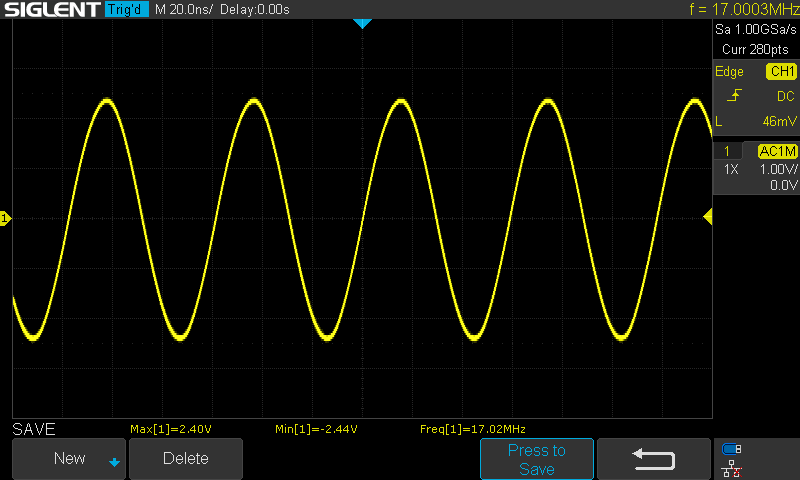
Figure 10 - 17 MHz Output High Amplitude
While the minimum amplitude at 17 MHz is 150mVp-p. We can also observe that the output is not perfectly centered around DC but slightly above 0V.
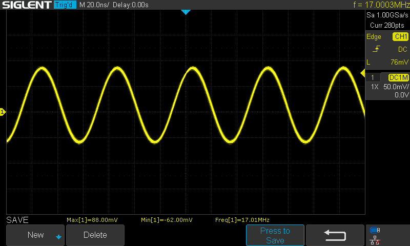
Figure 11 - 17 MHz Output Low Amplitude
Triangle Wave
The triangle wave output looked good as well. We can switch between filters to observe how filter group delay affects the triangle wave. The effects from the non-constant group delay of the elliptic filter should be visible as ripples in the high to low and low to high transitions. With a 3.6 MHz triangle wave, the 5th harmonic will be at 18 MHz so the aberrations we expect should be visible. These aberration are caused from the non-constant group delay vs. frequency properties of the filter so the harmonics of the triangle wave have different time delays.

Figure 12 - Triangle Wave Through Linear Phase Filters
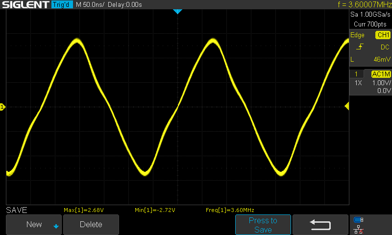
Figure 13 - Triangle Wave Through Elliptic Filters
Square Wave
Finally, the square wave output from the comparator was tested. The square wave output from pin 16 SIGN BIT OUT should have an amplitude from 0V to 3.3V (DVDD). Per the datasheet, the square wave input at pin 17 VIN should be a filtered sine wave with amplitude of 100mVp-p to 1Vp-p and frequency greater than 3 MHz in order for the ac-coupling to not affect the zero crossing detector.
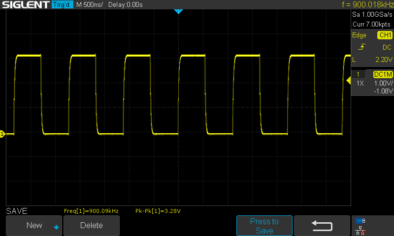
Figure 14 - 900 kHz Square Wave Output
When the amplitude was varied, the duty cycle of the square wave output also changed. At high frequencies, the output behaved like an RC transient response.
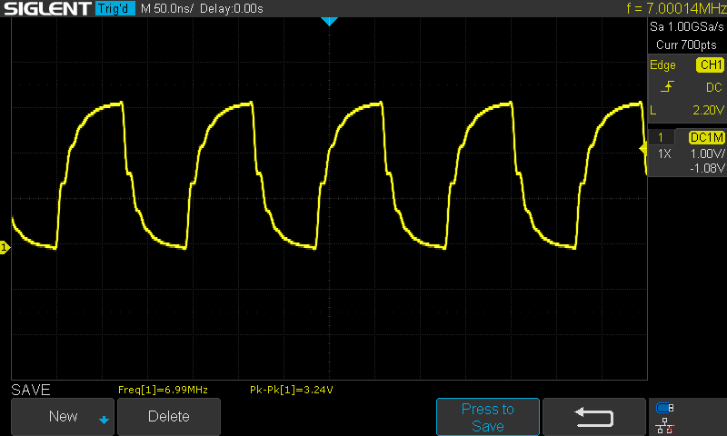
Figure 15 - Square Wave High Input Frequency
Phase and Frequency Modulation
We can also test the PSELECT and FSELECT pins to switch between phase and frequency registers, respectively.
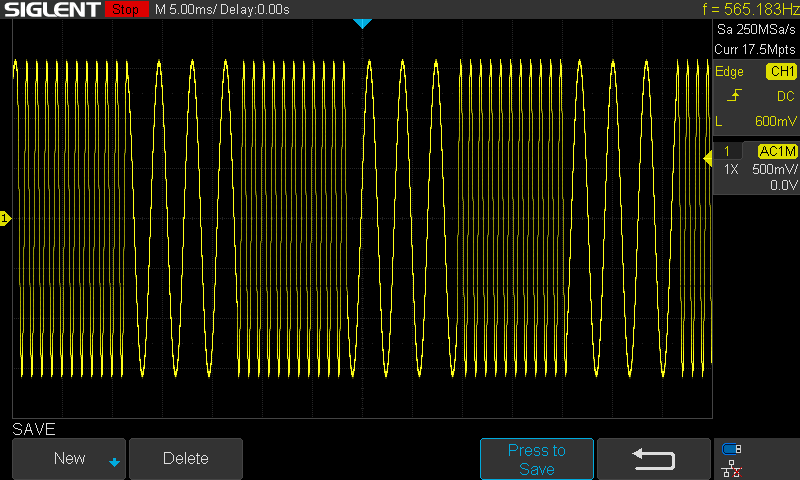
Figure 16 - Frequency Register Switching
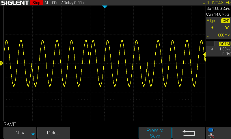
Figure 17 - Phase Register Switching
Supply Ripple
We can also measure the supply ripple to ensure a clean supply line is provided to the ICs.
There are 3 main power supply lines, the +5V, the -5V and the +3.3V. The +5V and -5V are for the analog components and the +3.3V is for the digital components. When measured with an oscilloscope probe and a ground spring, all three supply lines have around 1.4 mVp-p of ripple when the oscilloscope input is AC-coupled. However, I'm unsure how much of this ripple comes from the signal generator and how much from the measurement setup or oscilloscope.
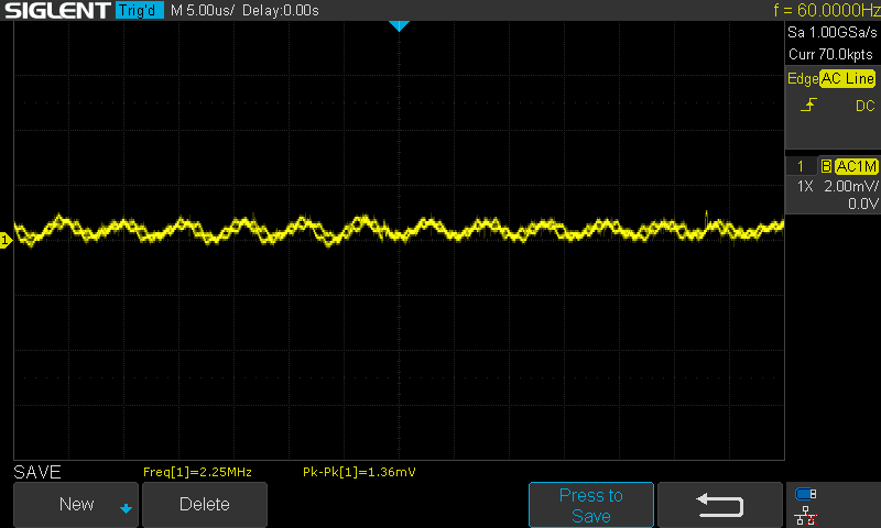
Figure 18 - Supply Ripple
Future Work
- Test output with spectrum analyzer to determine spurious free dynamic range of sine output.
- Try encoding data with BPSK or BFSK modulation by sending data on the PSELECT and FSELECT line so 0's and 1's can switch between phase or frequency registers.
- Fix DC offset so centered around 0V or allow user to change DC offset of output signal.
- Add more LEDs to indicate which filter is being used and if power supply sections are turned on.
