Overview:
- Design of a DDS based signal generator with a maximum sinusoidal output frequency of 17 MHz.
- Investigate and design an Elliptic low pass filter (LPF) and Equiripple Error Linear Phase LPF.
- Design of a low voltage ripple split power supply.
Table of Contents
- Introduction
- DDS Selection and Integration
- Filters and Output Amplifier
- Power Supply
- Final Schematic
- PCB Layout
- Future Work
Introduction
For my first project I wanted to design something useful that would also incorporate a few topics I wanted to better understand. One topic I want to better understand are Direct Digital Synthesis (DDS) ICs. These chips are able to create analog waveforms with very precise frequency and phase control. DDS ICs are used heavily in both communication and radar applications, which are both subjects I wish cover in future projects.
I also needed a signal generator for amplifier design work and wanted to learn how to use KiCAD, so I thought a simple signal generator PCB would be a great first project.
The KiCad project files can be found on GitHub.
DDS Selection and Integration
DDS Selection
The first requirement I had for my signal generator was to output a sine wave up to 20 MHz. Analog Devices recommends limiting the output frequency of a DDS to 1/3 of the reference clock frequency. So for an output frequency of 20 MHz, I'd need to find a DDS that operates with a minimum clock frequency of 60 MHz. Analog Devices AD9834 operates with a maximum clock frequency of 75 MHz and will easily meet my 20 MHz output frequency requirement. Unfortunately the 75 MHz version, AD9834CRUZ, was sold out and had a long lead time during the design of this project, so I settled with the 50 MHz versions, AD9834BRUZ. Using the 1/3 rule, the recommended frequency limit for the AD9834BRUZ is only 16.67 MHz but this will do for this project. The AD9834 can also output a triangle wave and incorporate a comparator which can be used to create square wave outputs.
DDS Integration
The AD9834 outputs its waveform through two complementary current output pins IOUT and IOUTB. AD9834 can be used in single-ended mode by only using one output pin or differential mode which we will be using in this design.
The load resistance must be chosen so that at the maximum voltage generated does not exceed the Output Compliance rating. For a maximum output current at 3mA and a load resistance of 200 ohms, a maximum output voltage of 0.6V will be generated which is below the AD9834 Output Compliance rating of 0.8V.
To minimize components in later stages I decided it would be best to change the differential outputs to single ended. This can be done with a balun but I also wanted to amplify the waveform before filtering so I chose an op-amp differential amplifier. The basic op-amp differential amplifier is given by the following circuit.

Figure 1 - Op Amp Differential Amplifier
If R1 = R2 and R3 = R4 then the output voltage becomes [1],
$$ V_{out} = \frac{R_3}{R_1}(V_2 - V_1) $$
The LT1818 op-amp was chosen because it provided adequate gain-bandwidth product, slew rate and output current to a 50 ohm load. A feedback capacitor C38 was added to improve stability per the manufacturer's recommendations.
If the differential amplifier discussed above was connected directly to the AD9834 outputs IOUT and IOUTB, the desired load resistance of 200 ohms would differ for each pin and cause non-complementary behavior at the outputs. To prevent this, emitter-followers were used as buffers to present near identical loads for the two output ports. The emitter resistor was chosen to not be too low to consume excessive power and not too high to cause clipping at the emitter output (due to emitter not being able to sink additional current and shutting off, see w2aew's explanantion).
Filters and Output Amplifier
Sine and Triangle Waves
The AD9834 outputs both a sinusoidal and triangular waveform. A single frequency sine wave in the time domain can be expressed as,
$$ s(t) = cos(2{\pi}ft) $$
From the frequency domain perspective this ideal single frequency sinusoid appears as a single spike at one frequency. For example, a 5 kHz sine wave in the frequency domain with some added white noise could appear as shown below, where the y-axis is the absolute value and the x-axis is frequency.
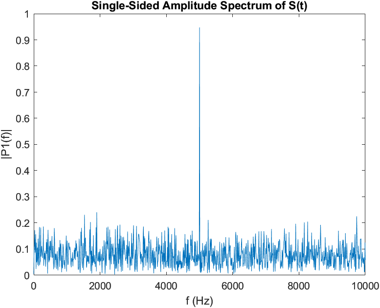
Figure 2 - 5 kHz Sine Wave with White Noise
On the other hand, the frequency spectrum of a 5 kHz triangular waveform includes multiple frequencies.
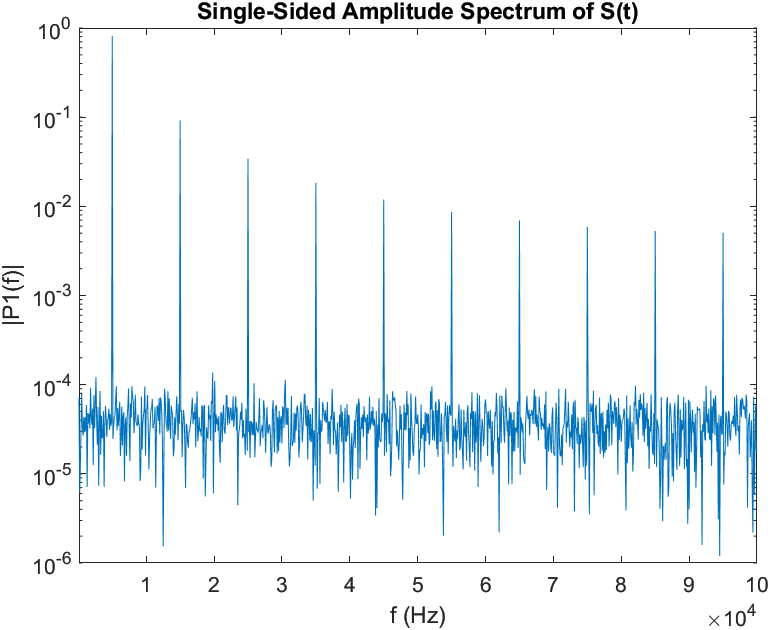
Figure 3 - 5 kHz Triangle Wave with White Noise
One way of expressing a triangle wave is as a sum of odd harmonics as shown below where \(n = 1, 3, 5\)... [2],
$$s(t) = \frac{8}{{\pi}^2} \sum \frac{(-1)^{(n-1)/2}}{n^2} sin(2{\pi}fnt)$$
This can be seen from it's power spectrum above that the triangle wave only includes odd order harmonics i.e 1st, 3rd, 5th, etc. in its spectrum.
What happens if we don't include all harmonics of the triangle wave? We can determine this graphically from the figure below where the legend show the number of harmonics included in each waveform. We can see that the waveform with only the first harmonic resembles a perfect sine wave while adding more harmonics cause the waveform to look more triangular.
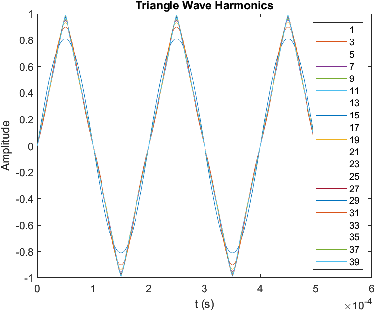
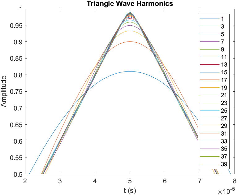
Figure 4 - Triangle Wave Incrementing Orders
For the purpose of this simple signal generator, we'll ensure to keep up to the 7th harmonic of the triangle wave.
9th Order Elliptic Filter
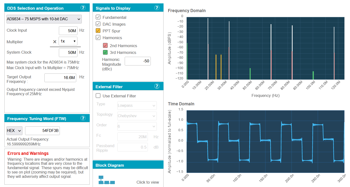
A DDS cannot produce an ideal single frequency sine wave. Instead, it outputs your desired frequency along with harmonics, spurs and image frequencies. This characteristic can be seen in Analog Devices ADIsimDDA web tool.
Figure 5 - DDS Output without Filtering
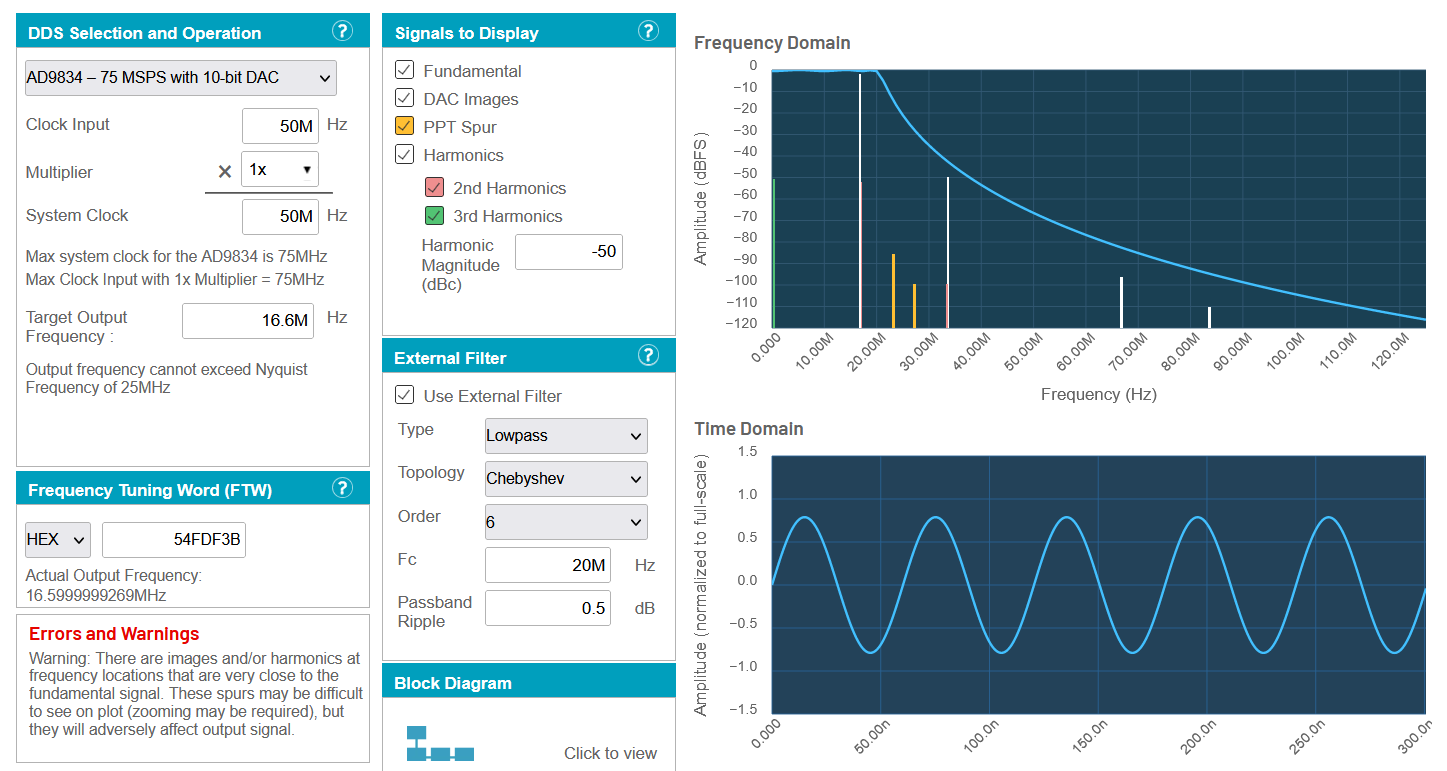
We find that without any filtering, discrete step become noticeable on the sine wave output at around 500 kHz due to significant power in the harmonics and spurs. But with external filtering, we can achieve the 16.6 MHz sine wave output easily.
Figure 6 - DDS Output with Filtering
Now that we know filtering is required to achieve a wide range of output frequencies we can choose the type of filter. There are many families of filters such as Bessel, Butterworth, Chebyshev, and so on which all make trade-offs between attenuation steepness, flatness of delay and passband ripple. For a sinusoidal output with only one frequency component, phase properties are not critical, so a filter with a steep rolloff and minimal ripple is what we're looking for. We must also remember that the first image frequency of a DDS occurs at,
$$ f_{first image} = f_{reference clock} - f_{out} $$
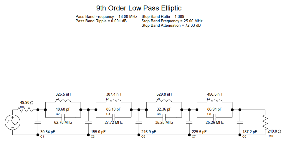
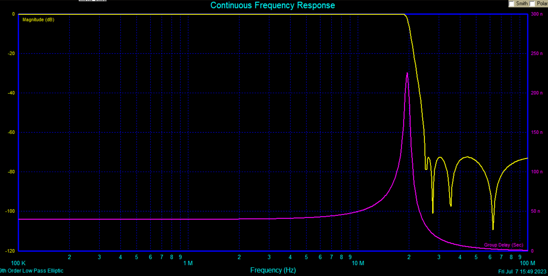
So as our output frequency increases, the first image frequency decreases. To ensure a proper sinusoidal output our filter must be steep enough to provide enough attenuation to that first image frequency without attenuating our desired frequency. With this in mind, I chose a 9th order Elliptic filter with a cutoff frequency of 18 MHz. I chose a larger load resistor compared to the source resistor to keep the output voltage high so the output amplifier does not need to have a high voltage gain. The filter was designed using a free version of Filter Solutions by Nuhertz Technologies which was downloaded from the resources of Analog Filter and Circuit Design Handbook.
Figure 7 - 9th Order Elliptic Filter
7th Order Linear Phase Filter
A few other characteristics must be considered when filtering a triangular waveforms. Because triangle waves need odd order harmonics, the attenuation steepness should not be too sharp to remove its higher order harmonics. We also must consider the delay of these higher order harmonics and ensure the delay is constant for all significant harmonics. To accomplish this, we must use a filter with a constant group delay over the frequency range of significant harmonics. A constant group delay is achieved when the filter has a linear phase response. Group delay \(\tau_{group delay}\) and phase response \(\theta(\omega)\) are related as follows:
$$\tau_{group delay} = - \frac{d\theta(\omega)}{d\omega}$$
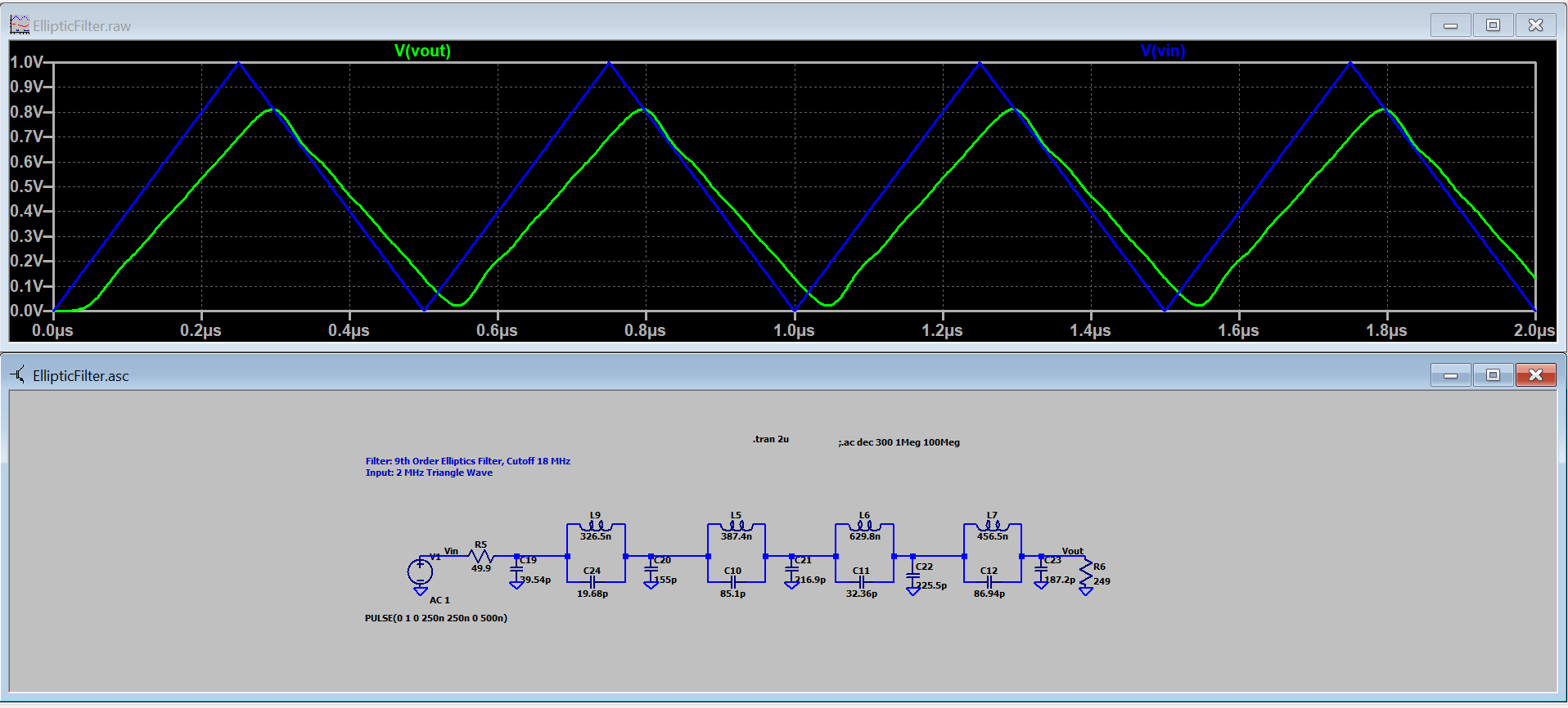
What happens if a triangle wave is filtered by a non-linear phase response filter. Well the harmonics begin to add out of phase and cause distortions in the triangle waveform. For example, when a 2 MHz triangle wave is filtered using the 9th order elliptic filter from the previous section, the outputs would look like below.
Figure 8 - 9th Order Elliptic Filter with Triangle Wave Input
From the simulation above we can see the tops and bottoms of the triangle wave at Vout are rounded due to the attenuation of the harmonics, but there are also aberrations in the transitions from low to high caused by the non-constant group delay presented to the harmonics.
The easiest way to design a linear phase LPF is to use a normalized prototype then scale the terminating resistors and cutoff frequency. An explanation on filter design using this method can be read in the LC Filter Design Using Normalized Prototypes post. A 7th order 0.05 degree ripple normalized prototype filter from the Handbook of Filter Synthesis [3] was scaled for a cutoff frequency of 10 MHz and will be used to filter the triangle output from the DDS chip.
Filter Switching Mechanism
With two separate filters for the two different output waveforms a Single Pole Double Throw (SPDT) relay is required to switch between filters.
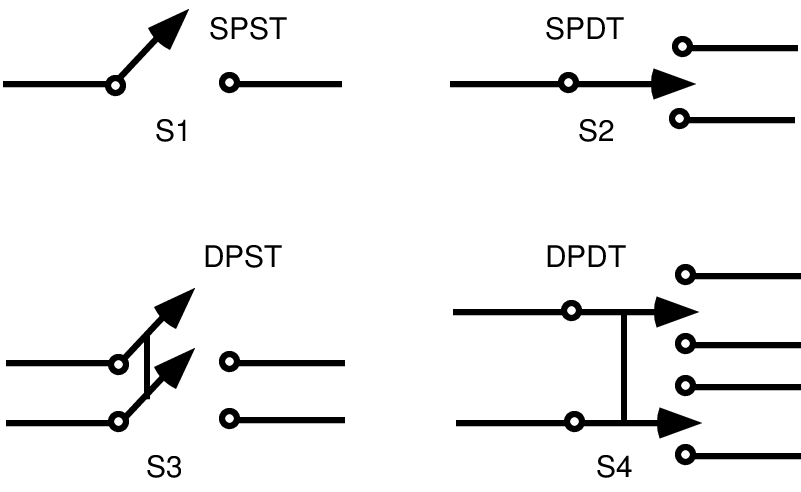
Figure 9 - Types of Switches
This will allow us to switch between filters depending on the output waveform of the AD9834. Relays often employ a coil which allow the operator to change between output pins when the coil is energized in a particular polarity. Because each filter could be used for a prolonged period, I decided to use a latching relay which once set, stays connected to our desired contact until changed. Non-latching relays require a constant voltage applied to the coil to set/reset the armature and therefore consumes power when idle.
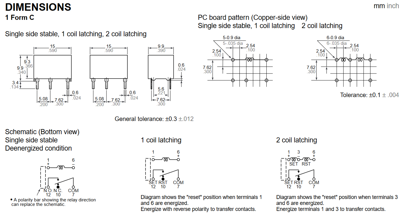
Most latching 5V or 3V relays were sold out at the time of design but I was able to find a 1 coil latching relay DS1E-SL-DC5V from Panasonic. In order to set this relay so the common pin (Pin 7) is connected to the set pin (Pin 12), a +8V to +4V voltage is required to be present across Pins 1 and 6. To connect the common pin to the reset pin (Pin 10), we'd simply present the same voltage but of opposite polarity across the coil.
Figure 10 - DS1E-SL-DC5V Relay
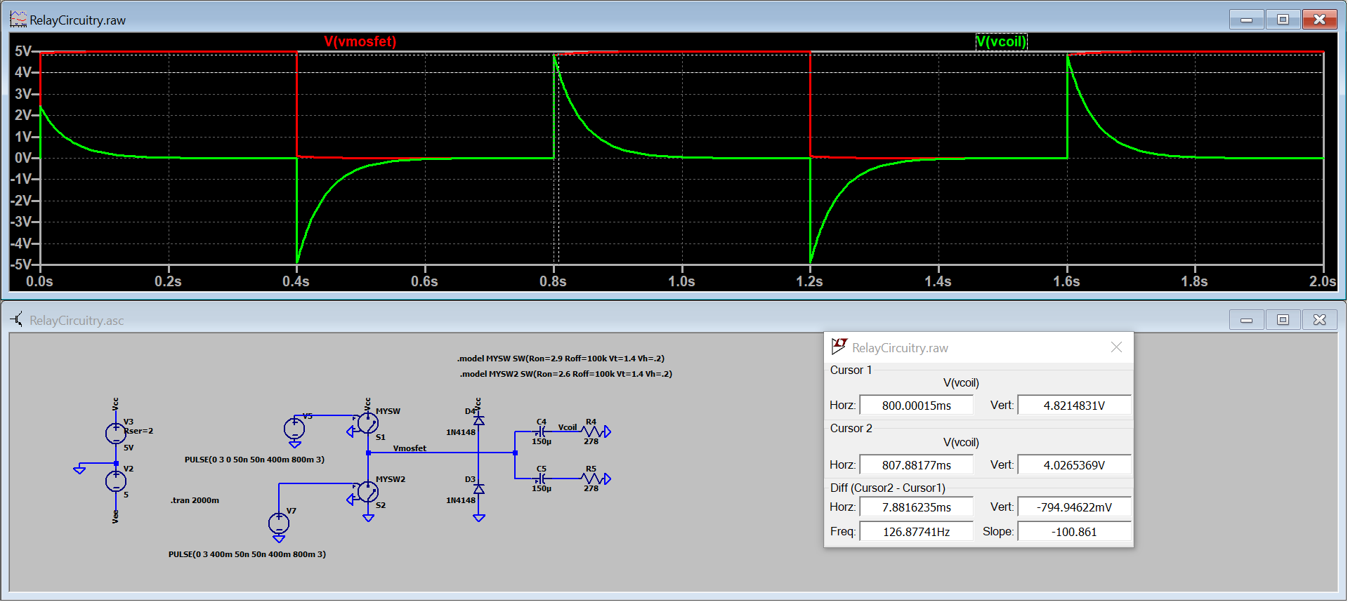
One way to set and reset this relay would be to set one side of the coil to ground and change the other side to +5V and -5V, but most microcontrollers don't output +5V or -5V so some intermediary circuitry would be required to be able to set/reset this relay with a microcontroller GPIO pin (usually LO=0V and HI=3.3V). The simplest approach I found is the switching mechanism described by Kerry Wong. This method allows you to simulate the +5V and -5V output with only a 0V to 5V driver. This method places a capacitor in series with the latching relay coil so when the driver goes from 0V to +5V the capacitor output will become +5 V temporarily but when the driver goes from +5V to 0V the capacitor output will be -5V temporarily. All latching relays have a minimum set/reset time that the voltage must be the applied to the coil. To accommodate long set/reset requirements, larger series capacitors can be used to slow the voltage decay.
To create the fast switching 0V to +5V and +5V to 0V signal, I used the MOSFET gate driver MCP14A0602 which can easily be controlled by a microcontroller GPIO pin.
Figure 11 - Switching Mechanism
DDS Output Amplifier
The purpose of the output amplifier is to provide sufficient power to a range of loads. The LT1816 was chosen because it still had a large Gain-Bandwidth product to provide some voltage gain but better output current characteristics than the LT1818 used as in the differential amplifier. A non-inverting op-amp configuration was chosen with a voltage gain of 2. The two parallel 100 ohm resistors provide a 50 ohm output impedance and allows the output current to be distributed between two resistors.
Power Supply
The power supply design is based on an Altium video created by Mark Harris. Slight adjustments were necessary to the design due to differences in input voltage and current draw. The component values for the switching regulator MAX17580ATC+ were all calculated using the equations from the datasheet.
A 3.3V linear regulator, ADP151AUJZ-3.3-R7, was added to design to supply power to the digital components. This separation between analog power and digital power allow less switching noise from the TXCO or AD9834 I/O pins from being added to our analog output. A ferrite bead with a max impedance centered close to a third of the TXCO rise time has also been added to minimize high frequency noise from the clock.
The values of the capacitors placed near active devices were determined by their datasheet recommendations.
Final Schematic
The finals schematic for the DDS signal generator is shown below:
PCB Layout
General PCB Considerations
An unbroken return plane was placed directly underneath the signal lines (top plane) to ensure tight field lines and reduce crosstalk.
Test points were added throughout the layout to be able to debug the design if troubleshooting was necessary and to view the signal at different stages of the design. These test points allow us to easily verify the power supply circuitry is working correctly, measure noise on the supply lines and ensure the filter switching circuitry is working correctly. Each test point has its own ground test point so the oscilloscope probe ground spring can be used when measuring. This allows for more accurate measuring by minimizing that ground inductance loop.
Also, for through-hole components connected to the large ground planes, thermal relief connections were used to make it easier to solder the components. With thermal reliefs, it does not take as long to melt the solder because less heat is dissipated to the two large ground planes.
Voltage planes were not required due to limited components requiring power and small current draw from these components. However, wide traces were used for voltage lines to ensure low inductance.
Return vias were placed near signals lines that were switching from layer 1 to 4 or vice versa to ensure low impedance return path.
Decoupling capacitors were placed as close to \(V_{in}\) pins as possible to minimize current loops. While this might not be necessary for this design because most signals are relatively low frequency it is a good habit.
A 4 layer PCB stackup was chosen because it allows the layout to have an unbroken return plane for signal lines, tighter coupling of EM fields due to shorter distance between signal and return plane and it does not cost much more for a 4 layer PCB compared to a 2 layer PCB.
Analog Waveform Considerations
The highest output frequency from the DDS will be around 17 MHz, therefore many high frequency layout considerations can be ignored because most interconnects will be electrically small. The wavelength in a microstrip transmission line is [4],
$$ \lambda = \frac{c}{f\sqrt{{\epsilon}_{eff}}} $$
where,
$$ \epsilon_{eff} = \frac{\epsilon_{r} + 1}{2} + \frac{\epsilon_{r} - 1}{2} \frac{1}{\sqrt{1 + 12d/W}} $$
Using JLCPCB Prepreg 3313 and JLCPCB Stackup JLC04161H-3313, the relative dielectric constant, \(\epsilon_r\), is 4.05, the distance between trace and return plane, \(d\), is 0.0994 mm and the width of the trace, \(W\), will be 0.6 mm therefore the effective dielectric constant,\(\epsilon_{eff}\), is 3.41. For a 17 MHz signal the effective wavelength in the microstrip transmission line is 9.6 meters.
Using the rule of thumb that if interconnects are less than \(\frac{\lambda}{20}\), impedance control can be ignored then as long as we keep interconnects less than 48 cm we don't have to worry about impedance matching and impedance control. In the design, all analog interconnects are less than 48 cm.
Analog sections have also been physically separated from the Digital I/O and Power Supply sections to try to minimize noise coupling to the output waveform.
Final PCB Layout
The finals PCB layout for the DDS signal generator is shown below:
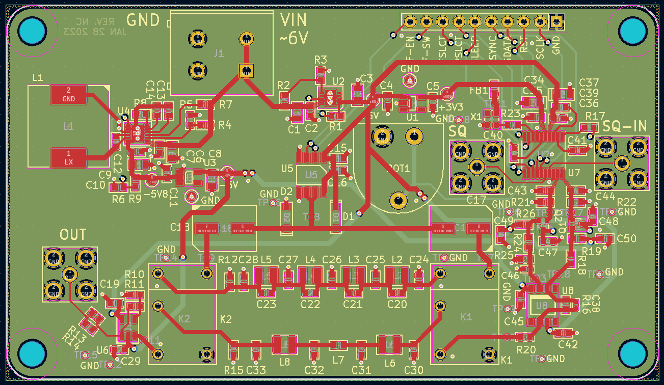
Figure 12 - Final PCB Layout
Future Work
- More power efficient buffer stage. Design a stage that does not draw current when no output present.
- Adjust filters to reverse effects of sinx/x rolloff from DDS.
References
[1] Electronics Tutorials, https://www.electronics-tutorials.ws/opamp/opamp_5.html
[2] Weisstein, Eric W. "Triangle Wave." From MathWorld--A Wolfram Web Resource. https://mathworld.wolfram.com/TriangleWave.html
[3] Anatol I. Zverev, Handbook of Filter Synthesis, 1967, https://ia803101.us.archive.org/20/items/HandbookOfFilterSynthesis/Handbook%20of%20Filter%20Synthesis.pdf
[4] Pozar, David M. Microwave Engineering 4th Edition, 2011
